- 您現(xiàn)在的位置:買賣IC網(wǎng) > PDF目錄8621 > MAX3654ETE+ (Maxim Integrated Products)IC AMP TRANSIMPEDANCE 16-TQFN PDF資料下載
參數(shù)資料
| 型號: | MAX3654ETE+ |
| 廠商: | Maxim Integrated Products |
| 文件頁數(shù): | 7/8頁 |
| 文件大小: | 0K |
| 描述: | IC AMP TRANSIMPEDANCE 16-TQFN |
| 產(chǎn)品培訓(xùn)模塊: | Lead (SnPb) Finish for COTS Obsolescence Mitigation Program |
| 標(biāo)準(zhǔn)包裝: | 75 |
| 類型: | 轉(zhuǎn)阻放大器 |
| 應(yīng)用: | CATV |
| 安裝類型: | 表面貼裝 |
| 封裝/外殼: | 16-WQFN 裸露焊盤 |
| 供應(yīng)商設(shè)備封裝: | 16-TQFN-EP(4x4) |
| 包裝: | 管件 |

MAX3654
47MHz to 870MHz Analog CATV
Transimpedance Amplifier
_______________________________________________________________________________________
7
Applications Information
Photodiode Parasitics
The MAX3654 TIA is designed to operate with a low-
capacitance analog photodiode. Proper system design
includes considerations of lead configuration, pad, and
through-hole geometry, and PC board layer selection for
connections to the IC. The TIA is designed to operate
correctly when the total capacitance of the photodiode,
package, leads and PC board is between 1.0pF and
2.5pF.
RF Output
The differential TIA RF output should be connected
(AC-coupled) to a balun transformer for normal single-
ended output.
AGC Operation
For AGC operation, the optical average power can be
measured from the voltage drop across the lower bias
resistor, using high impedance to isolate the photodi-
ode as shown in the EV kit schematic. TIA gain is
inversely proportional to the voltage present at VAGC
from 0.175V to 1.4V. From 0 to 0.175V, the gain is con-
stant and maximum. The nominal gain is given by:
When connected as shown in the Typical Applications
Circuit, the MAX3654 will maintain the electrical output
constant (15dBmV/ch) for optical signals in the
-6dBm to +2dBm range.
Evaluation Kit and PC Board Layout
The factory-assembled EV kit for the MAX3654 pro-
vides two versions: optical input and electrical input.
The optical input circuit includes photodiode bias cir-
cuitry, an op amp to adjust VAGC according to the DC
photodiode current (for AGC operation), an output
balun, and a 75
output connector. Through-hole pads
are provided to attach the triplexer analog photodiode
leads. Since photodiode capacitance and package
lead inductance affect the amount of uptilt, in configu-
rations where lead inductance is significantly lower
than the value shown in Figure 2, the uptilt may be
increased by providing discrete inductance on the PC
board. When a CPD = 0.5pF (typ) photodiode is mount-
ed with 5mm (nominal) leads into through-hole vias as
in the EV kit configuration, a 4dB uptilt will normally be
achieved. It is important to configure the layout with
capacitance and inductance in the anode and cathode
connection as symmetric as possible.
The electrical input circuit is normally configured with a
50
input for use with conventional test and measure-
ment equipment. If desired, the MAX3654 input can
also be terminated with 75
as shown in the EV kit data
sheet. The 75
EV kit outputs should be connected to
50
test and measurement equipment using a mini-
mum loss pad.
For more information, see the Maxim website:
MAX3654 EV Kit data sheet—
http://www.maxim-ic.com/Fiber.cfm
Minimum Loss Pad—
http://www.maxim-ic.com/appnotes.cfm/appnote_number/972
ZT dB
dB
mV
VAGC mV
V
VAGC
V
()
log
()
(.
.
).
=+
×
≤≤
62
20
175
0 175
1 4
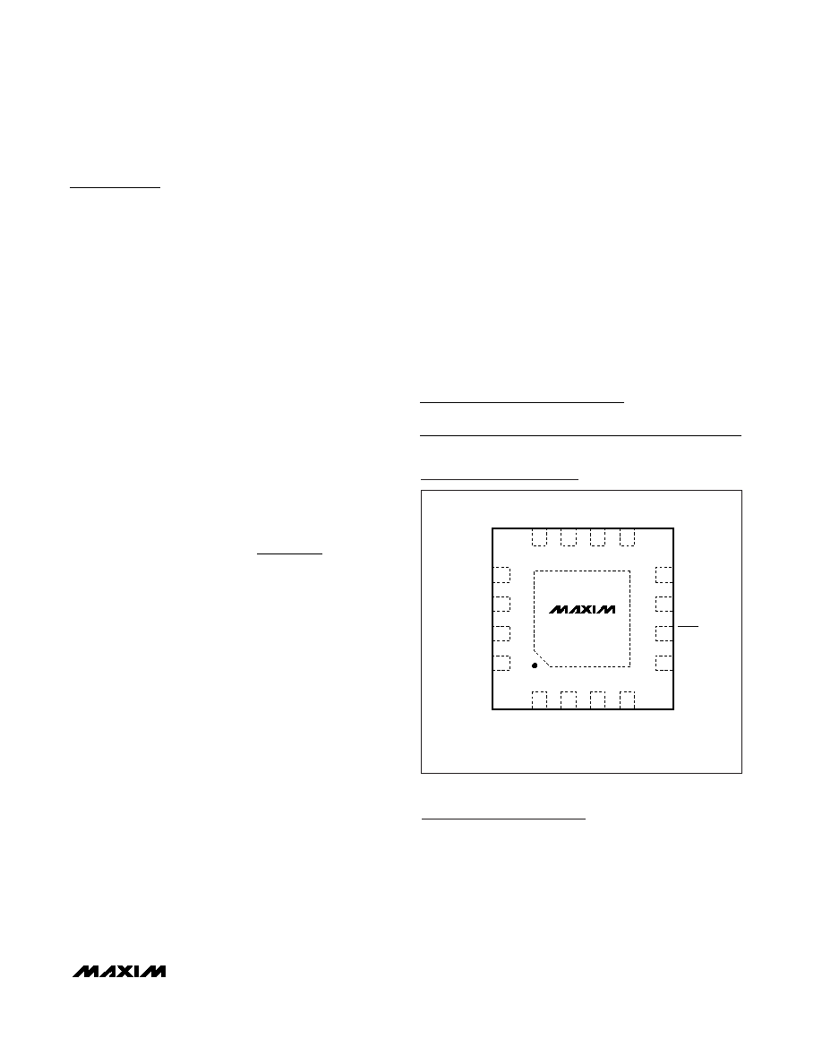
Chip Information
TRANSISTOR COUNT: 3376
PROCESS: SiGe Bipolar
SUBSTRATE: SOI
15
16
14
13
6
5
7
IN+
V
CC
8
V
CC
OUT+
V
CC
V
CC
12
GND
4
12
11
9
TEST2
GND
EP*
HYST
MUTE
VAGC
MAX3654
IN-
OUT-
3
10
TEST1
THIN QFN
4mm x 4mm
TOP VIEW
Pin Configuration
*THE EXPOSED PAD MUST BE
CONNECTED TO GROUND.
相關(guān)PDF資料 |
PDF描述 |
|---|---|
| LTC2753ACUK-16#TRPBF | IC DAC 16BIT DUAL 48-QFN |
| DAC8800FSZ-REEL | IC DAC 8BIT OCTAL CMOS 20SOIC |
| VE-25M-IV-F3 | CONVERTER MOD DC/DC 10V 150W |
| VE-25M-IV-F1 | CONVERTER MOD DC/DC 10V 150W |
| VE-251-IV-F3 | CONVERTER MOD DC/DC 12V 150W |
相關(guān)代理商/技術(shù)參數(shù) |
參數(shù)描述 |
|---|---|
| MAX3654ETE+ | 功能描述:跨阻抗放大器 47-870MHz Alog CATV Transimpedance Amp RoHS:否 制造商:Texas Instruments 封裝 / 箱體:SOIC-14 帶寬:3 MHz 工作電源電壓:36 V 電源電流:5.5 mA 工作溫度范圍:- 40 C to + 85 C 封裝:Tube |
| MAX3654ETE+T | 功能描述:跨阻抗放大器 47-870MHz Alog CATV Transimpedance Amp RoHS:否 制造商:Texas Instruments 封裝 / 箱體:SOIC-14 帶寬:3 MHz 工作電源電壓:36 V 電源電流:5.5 mA 工作溫度范圍:- 40 C to + 85 C 封裝:Tube |
| MAX3654EVKIT | 功能描述:跨阻抗放大器 MAX3654 Evaluation Kit RoHS:否 制造商:Texas Instruments 封裝 / 箱體:SOIC-14 帶寬:3 MHz 工作電源電壓:36 V 電源電流:5.5 mA 工作溫度范圍:- 40 C to + 85 C 封裝:Tube |
| MAX3656E/D | 功能描述:激光驅(qū)動器 RoHS:否 制造商:Micrel 數(shù)據(jù)速率:4.25 Gbps 工作電源電壓:3 V to 3.6 V 電源電流:80 mA 最大工作溫度:+ 85 C 封裝 / 箱體:QFN-16 封裝:Tube |
| MAX3656ETA | 制造商:Maxim Integrated Products 功能描述:- Rail/Tube |
發(fā)布緊急采購,3分鐘左右您將得到回復(fù)。