- 您現(xiàn)在的位置:買賣IC網(wǎng) > PDF目錄385552 > MAX820 (Maxim Integrated Products, Inc.) Microprocessor and Non-Volatile Memory Supervisory Circuits PDF資料下載
參數(shù)資料
| 型號(hào): | MAX820 |
| 廠商: | Maxim Integrated Products, Inc. |
| 英文描述: | Microprocessor and Non-Volatile Memory Supervisory Circuits |
| 中文描述: | 微處理器及非易失存儲(chǔ)器監(jiān)控電路 |
| 文件頁(yè)數(shù): | 13/16頁(yè) |
| 文件大?。?/td> | 250K |
| 代理商: | MAX820 |
第1頁(yè)第2頁(yè)第3頁(yè)第4頁(yè)第5頁(yè)第6頁(yè)第7頁(yè)第8頁(yè)第9頁(yè)第10頁(yè)第11頁(yè)第12頁(yè)當(dāng)前第13頁(yè)第14頁(yè)第15頁(yè)第16頁(yè)
M
Mic roproc essor and Non-Volatile
Memory S upervisory Circ uits
______________________________________________________________________________________
13
Chip-Enable S ignal Gating
The MAX792/MAX820 provide internal gating of chip-
enable (CE) signals, which prevents erroneous data
from corrupting CMOS RAM in the event of an under-
voltage condition. The MAX792/MAX820 use a series
transmission gate from
CE
IN to
CE
OUT (Figure 1).
During normal operation (reset not asserted), the CE
transmission gate is enabled and passes all CE transi-
tions. When reset is asserted, this path becomes dis-
abled, preventing erroneous data from corrupting the
CMOS RAM. The 10ns max CE propagation delay from
CE
IN to
CE
OUT enables the MAX792/MAX820 to be
used with most μPs. If
CE
IN is low when reset asserts,
CE
OUT remains low for a short period to permit com-
pletion of the current write cycle.
Chip-Enable Input
The CE transmission gate is disabled and
CE
IN is high
impedance (disabled mode) while reset is asserted.
During a power-down sequence when V
CC
passes the
reset threshold, the CE transmission gate disables and
CE
IN immediately becomes high impedance if the volt-
age at
CE
IN is high. If
CE
IN is low when reset is assert-
ed, the CE transmission gate will disable at the moment
CE
IN goes high or 15μs after reset is asserted,
whichever occurs first (Figure 9). This permits the cur-
rent write cycle to complete during power-down.
During a power-up sequence, the CE transmission gate
remains disabled and
CE
IN remains high impedance
regardless of
CE
IN activity, until reset is deasserted fol-
lowing the reset timeout period.
While disabled,
CE
IN is high impedance. When the CE
transmission gate is enabled, the impedance of
CE
IN
will appear as a 75
(V
CC
= 5V) resistor in series with
the load at
CE
OUT.
The propagation delay through the CE transmission
gate depends on V
CC,
the source impedance of the
drive connected to
CE
IN, and the loading on
CE
OUT
(see the Chip-Enable Propagation Delay vs.
CE
OUT
Load Capacitance graph in the Typical Operating
Characteristics). The CE propagation delay is produc-
tion tested from the 50% point on
CE
IN to the 50%
point on
CE
OUT using a 50
driver and 50pF of load
capacitance (Figure 10). For minimum propagation
delay, minimize the capacitive load at
CE
OUT, and use
a low-output-impedance driver.
Chip-Enable Output
When the CE transmission gate is enabled, the imped-
ance of
CE
OUT is equivalent to 75
in series with the
source driving
CE
IN. In the disabled mode, the 75
transmission gate is off and an active pull-up connects
from
CE
OUT to V
CC
. This source turns off when the
transmission gate is enabled.
Applic ations Information
Connect a 0.1μF ceramic capacitor from V
CC
to GND,
as close to the device pins as possible. This reduces
the probability of resets due to high-frequency power-
supply transients. In a high-noise environment, addi-
tional bypass capacitance from V
CC
to ground may be
required. If long leads connect to the chip inputs,
ensure that these lines are free from ringing, etc., which
would forward bias the chip’s protection diodes.
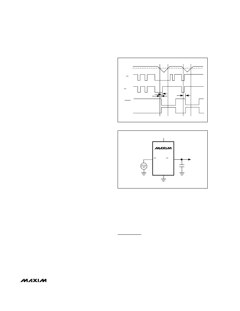
V
CC
CE IN
RESET
THRESHOLD
CE OUT
RESET
RESET
70
μ
s
15
μ
s
70
μ
s
Figure 9. Reset and Chip-Enable Timing
MAX792
MAX820
CE IN
50
DRIVER
13
14
12
+5V
GND
C
LOAD
3
V
CC
CE OUT
Figure 10. CE Propagation Delay Test Circuit
相關(guān)PDF資料 |
PDF描述 |
|---|---|
| MAX820_CPE | Microprocessor and Non-Volatile Memory Supervisory Circuits |
| MAX820_CSE | Microprocessor and Non-Volatile Memory Supervisory Circuits |
| MAX820_EJE | Microprocessor and Non-Volatile Memory Supervisory Circuits |
| MAX820_EPE | Microprocessor and Non-Volatile Memory Supervisory Circuits |
| MAX820_ESE | Microprocessor and Non-Volatile Memory Supervisory Circuits |
相關(guān)代理商/技術(shù)參數(shù) |
參數(shù)描述 |
|---|---|
| MAX820_CPE | 制造商:MAXIM 制造商全稱:Maxim Integrated Products 功能描述:Microprocessor and Non-Volatile Memory Supervisory Circuits |
| MAX820_CSE | 制造商:MAXIM 制造商全稱:Maxim Integrated Products 功能描述:Microprocessor and Non-Volatile Memory Supervisory Circuits |
| MAX820_EJE | 制造商:MAXIM 制造商全稱:Maxim Integrated Products 功能描述:Microprocessor and Non-Volatile Memory Supervisory Circuits |
| MAX820_EPE | 制造商:MAXIM 制造商全稱:Maxim Integrated Products 功能描述:Microprocessor and Non-Volatile Memory Supervisory Circuits |
| MAX820_ESE | 制造商:MAXIM 制造商全稱:Maxim Integrated Products 功能描述:Microprocessor and Non-Volatile Memory Supervisory Circuits |
發(fā)布緊急采購(gòu),3分鐘左右您將得到回復(fù)。