- 您現(xiàn)在的位置:買賣IC網(wǎng) > PDF目錄385552 > MAX820 (Maxim Integrated Products, Inc.) Microprocessor and Non-Volatile Memory Supervisory Circuits PDF資料下載
參數(shù)資料
| 型號: | MAX820 |
| 廠商: | Maxim Integrated Products, Inc. |
| 英文描述: | Microprocessor and Non-Volatile Memory Supervisory Circuits |
| 中文描述: | 微處理器及非易失存儲器監(jiān)控電路 |
| 文件頁數(shù): | 14/16頁 |
| 文件大?。?/td> | 250K |
| 代理商: | MAX820 |
M
Mic roproc essor and Non-Volatile
Memory S upervisory Circ uits
14
______________________________________________________________________________________
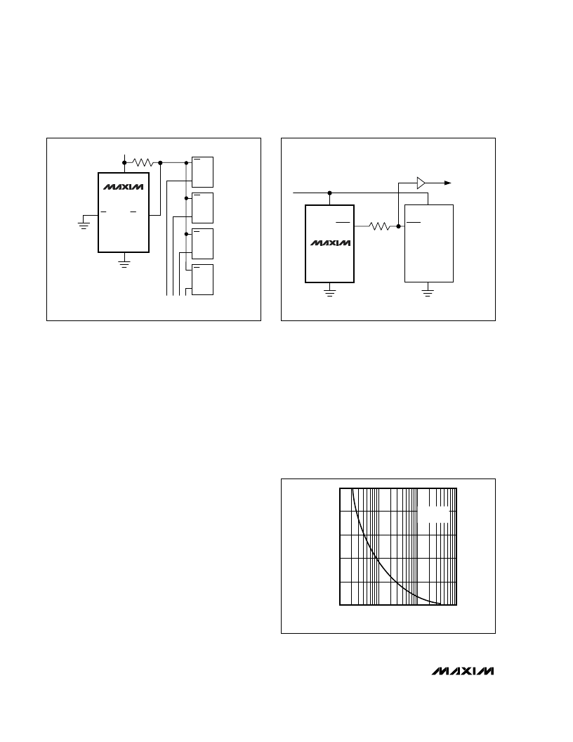
Alternative Chip-Enable Gating
Using memory devices with both CE and
CE
inputs
allows the MAX792/MAX820 CE propagation delay
to be bypassed. To do this, connect
CE
IN to ground,
pull up
CE
OUT to V
CC
, and connect
CE
OUT to the
CE
input of each memory device (Figure 11). The CE input
of each memory device then connects directly to the
chip-select logic, which does not have to be gated by
the MAX792/MAX820.
Interfac ing to μPs with Bidirec tional
Reset Inputs
μPs with bidirectional reset pins, such as the Motorola
68HC11 series, can contend with the MAX792/MAX820
RESET
output. If, for example, the MAX792/MAX820
RESET
output is asserted high and the μP wants to pull it low,
indeterminate logic levels may result. To avoid this,
connect a 4.7k
resistor between the MAX792/MAX820
RESET
output and the μP reset I/O, as in Figure 12.
Buffer the MAX792/MAX820
RESET
output to other sys-
tem components.
Negative-Going V
CC
T ransients
While issuing resets to the μP during power-up, power-
down, and brownout conditions, these supervisors are
relatively immune to short-duration negative-going V
CC
transients (glitches). It is usually undesirable to reset
the μP when V
CC
experiences only small glitches.
Figure 13 shows maximum transient duration vs. reset-
comparator overdrive, for which reset pulses are
not
generated. The graph was produced using negative-
going V
CC
pulses, starting at 5V and ending below the
reset threshold by the magnitude indicated (reset-
comparator overdrive). The graph shows the maximum
pulse width a negative-going V
CC
transient may typi-
cally have without causing a reset pulse to be issued.
As the amplitude of the transient increases (i.e., goes
farther below the reset threshold), the maximum allow-
able pulse width decreases. Typically, a V
CC
transient
that goes 100mV below the reset threshold and lasts for
30μs or less will not cause a reset pulse to be issued.
A 100nF bypass capacitor mounted close to the V
CC
pin provides additional transient immunity.
MAX792
MAX820
CE IN
13
14
12
+5V
GND
3
V
CC
CE OUT
CE
CE
CE
CE
CE
CE
CE
CE
RAM 1
RAM 2
RAM 3
RAM 4
ACTIVE-HIGH CE
LINES FROM LOGIC
MAXIMUM R
P
VALUE DEPENDS ON
THE NUMBER OF RAMS.
MINIMUM R
P
VALUE IS 1k
*
R
P
*
Figure 11. Alternate CE Gating
V
CC
V
CC
V
CC
μ
P
BUFFER
TOOTHER
SYSTEM RESET
INPUTS
4.7k
1
RESET
RESET
GND
GND
12
MAX792
MAX820
3
Figure 12. Interfacing to μPs with Bidirectional
RESET
Pins
Figure 13. Maximum Transient Duration without Causing a
Reset Pulse vs. Reset-Comparator Overdrive
100
0
10
100
10,000
40
20
80
60
M
RESET COMPARATOR OVERDRIVE, (V
TH
- V
CC
) (mV)
M
1000
V
CC
= 5V
T
A
= +25°C
相關(guān)PDF資料 |
PDF描述 |
|---|---|
| MAX820_CPE | Microprocessor and Non-Volatile Memory Supervisory Circuits |
| MAX820_CSE | Microprocessor and Non-Volatile Memory Supervisory Circuits |
| MAX820_EJE | Microprocessor and Non-Volatile Memory Supervisory Circuits |
| MAX820_EPE | Microprocessor and Non-Volatile Memory Supervisory Circuits |
| MAX820_ESE | Microprocessor and Non-Volatile Memory Supervisory Circuits |
相關(guān)代理商/技術(shù)參數(shù) |
參數(shù)描述 |
|---|---|
| MAX820_CPE | 制造商:MAXIM 制造商全稱:Maxim Integrated Products 功能描述:Microprocessor and Non-Volatile Memory Supervisory Circuits |
| MAX820_CSE | 制造商:MAXIM 制造商全稱:Maxim Integrated Products 功能描述:Microprocessor and Non-Volatile Memory Supervisory Circuits |
| MAX820_EJE | 制造商:MAXIM 制造商全稱:Maxim Integrated Products 功能描述:Microprocessor and Non-Volatile Memory Supervisory Circuits |
| MAX820_EPE | 制造商:MAXIM 制造商全稱:Maxim Integrated Products 功能描述:Microprocessor and Non-Volatile Memory Supervisory Circuits |
| MAX820_ESE | 制造商:MAXIM 制造商全稱:Maxim Integrated Products 功能描述:Microprocessor and Non-Volatile Memory Supervisory Circuits |
發(fā)布緊急采購,3分鐘左右您將得到回復(fù)。