- 您現(xiàn)在的位置:買賣IC網(wǎng) > PDF目錄69018 > MAX8893CEWV+ (MAXIM INTEGRATED PRODUCTS INC) SPECIALTY MICROPROCESSOR CIRCUIT, PBGA30 PDF資料下載
參數(shù)資料
| 型號(hào): | MAX8893CEWV+ |
| 廠商: | MAXIM INTEGRATED PRODUCTS INC |
| 元件分類: | 微控制器/微處理器 |
| 英文描述: | SPECIALTY MICROPROCESSOR CIRCUIT, PBGA30 |
| 封裝: | 3 X 2.50 MM, 0.64 MM HEIGHT, ROHS COMPLIANT, WLP-30 |
| 文件頁(yè)數(shù): | 24/51頁(yè) |
| 文件大?。?/td> | 4976K |
| 代理商: | MAX8893CEWV+ |
第1頁(yè)第2頁(yè)第3頁(yè)第4頁(yè)第5頁(yè)第6頁(yè)第7頁(yè)第8頁(yè)第9頁(yè)第10頁(yè)第11頁(yè)第12頁(yè)第13頁(yè)第14頁(yè)第15頁(yè)第16頁(yè)第17頁(yè)第18頁(yè)第19頁(yè)第20頁(yè)第21頁(yè)第22頁(yè)第23頁(yè)當(dāng)前第24頁(yè)第25頁(yè)第26頁(yè)第27頁(yè)第28頁(yè)第29頁(yè)第30頁(yè)第31頁(yè)第32頁(yè)第33頁(yè)第34頁(yè)第35頁(yè)第36頁(yè)第37頁(yè)第38頁(yè)第39頁(yè)第40頁(yè)第41頁(yè)第42頁(yè)第43頁(yè)第44頁(yè)第45頁(yè)第46頁(yè)第47頁(yè)第48頁(yè)第49頁(yè)第50頁(yè)第51頁(yè)
PMICs for Multimedia Application Processors
in a 3.0mm x 2.5mm WLP
MAX8893A/MAX8893B/MAX8893C
30 _____________________________________________________________________________________
Power-Up Sequencing
Drive ENBUCK or ENLDO_ high to turn on the BUCK
converter or the corresponding LDOs. When ENBUCK
and ENLDO_ are connected together and driven from
low to high, all the regulators are turned on with the
preset power-up sequencing. There are time delays
between each regulator to limit input current rush.
The MAX8893A/MAX8893B/MAX8893C have different
power-up time delays between each regulator. See the
Typical Operating Characteristics for details.
Undervoltage Lockout
When VIN rises above the undervoltage lockout thresh-
old (2.85V typ), the MAX8893A/MAX8893B/MAX8893C
can be enabled by driving any EN_ high or ENUSB
low. The UVLO threshold hysteresis is typically 0.5V.
Therefore, if VIN falls below 2.35V (typ), the undervolt-
age lockout circuitry disables all outputs and all internal
registers are reset to default values.
Reference Noise Bypass (REFBP)
Bypass REFBP to AGND with a 0.1FF ceramic capaci-
tor to reduce noise on the LDO outputs. REFBP is high
impedance in shutdown.
Thermal-Overload Protection
Thermal-overload protection limits total power dissi-
pation in the MAX8893A/MAX8893B/MAX8893C. The
step-down converter and LDOs have independent ther-
mal protection circuits. When the junction temperature
exceeds +160NC, the LDO, or step-down thermal-
overload protection circuitry disables the corresponding
regulators, allowing the IC to cool. The LDO thermal-
overload protection circuit enables the LDOs after the
LDO junction temperature cools down, resulting in
pulsed LDO outputs during continuous thermal-overload
conditions. The step-down converter’s thermal-overload
protection circuitry enables the step-down converter
after the junction temperature cools down. Thermal-
overload protection safeguards the IC in the event of
fault conditions.
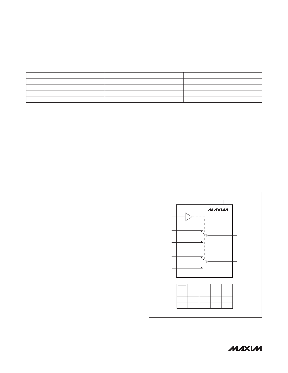
USB High-Speed Switch
The USB high-speed switch is a Q15kV ESD-protected
DPDT analog switch. It is ideal for USB 2.0 Hi-Speed
(480Mbps) switching applications and also meets USB
low- and full-speed requirements.
The USB switch is fully specified to operate from a single
2.7V to 5.5V supply. The switch is based on charge-pump-
assisted n-channel architecture. The switch also features a
shutdown mode to reduce the quiescent current.
Digital Control Input
The USB high-speed switch provides a single-bit control
logic input, CB. CB controls the position of the switches
as shown in Figure 7. Driving CB rail-to-rail minimizes
power consumption.
Table 4. Truth Table for USB Switch
Figure 7. USB Switch Functional Diagram/Truth Table
ENUSB
EUSB BIT
USB SWITCH
0
On
0
1
On
1
0
On
1
Off
CB
BATT
NO1
NC1
NO2
NC2
COM1
COM2
0
ENUSB
0
1
0
CB
1
X
OFF
N0_
ON
OFF
—
COM_
HI-Z
ON
NC_
OFF
X = DON'T CARE.
MAX8893A
MAX8893B
MAX8893C
ENUSB
相關(guān)PDF資料 |
PDF描述 |
|---|---|
| MAX9485ETP+ | 73.728 MHz, OTHER CLOCK GENERATOR, QCC20 |
| MAXQ1004-B01+ | RISC MICROCONTROLLER, QCC16 |
| MAXQ2010-RFX+ | 16-BIT, FLASH, 10 MHz, RISC MICROCONTROLLER, PQFP100 |
| MAXQ3120-FFN+ | 16-BIT, FLASH, 8 MHz, RISC MICROCONTROLLER, PQFP80 |
| MAXQ3120-FFN | 16-BIT, FLASH, 8 MHz, RISC MICROCONTROLLER, PQFP80 |
相關(guān)代理商/技術(shù)參數(shù) |
參數(shù)描述 |
|---|---|
| MAX8893CEWV+ | 制造商:Maxim Integrated Products 功能描述:UPMIC FOR APPLICATION PROCESSOR - Rail/Tube |
| MAX8893CEWV+T | 制造商:Maxim Integrated Products 功能描述:UPMIC FOR APPLICATION PROCESSOR - Tape and Reel |
| MAX8895EVKIT+ | 功能描述:電池管理 EVKIT for MAX8895 RoHS:否 制造商:Texas Instruments 電池類型:Li-Ion 輸出電壓:5 V 輸出電流:4.5 A 工作電源電壓:3.9 V to 17 V 最大工作溫度:+ 85 C 最小工作溫度:- 40 C 封裝 / 箱體:VQFN-24 封裝:Reel |
| MAX8895VEWA+ | 制造商:Maxim Integrated Products 功能描述:LI-ION CHARGERS WITH SMART POWER SELECTOR, ADAPTER TYPE DETE - Rail/Tube |
| MAX8895VEWA+T | 制造商:Maxim Integrated Products 功能描述:LI-ION CHARGERS WITH SMART POWER SELECTOR, ADAPTER TYPE DETE - Tape and Reel |
發(fā)布緊急采購(gòu),3分鐘左右您將得到回復(fù)。