- 您現(xiàn)在的位置:買賣IC網(wǎng) > PDF目錄10625 > MAX9123EUE+ (Maxim Integrated Products)IC INTERFACE PDF資料下載
參數(shù)資料
| 型號: | MAX9123EUE+ |
| 廠商: | Maxim Integrated Products |
| 文件頁數(shù): | 7/10頁 |
| 文件大小: | 0K |
| 描述: | IC INTERFACE |
| 產(chǎn)品培訓(xùn)模塊: | Obsolescence Mitigation Program |
| 標準包裝: | 96 |
| 系列: | * |
MAX9123
Quad LVDS Line Driver with
Flow-Through Pinout
6
_______________________________________________________________________________________
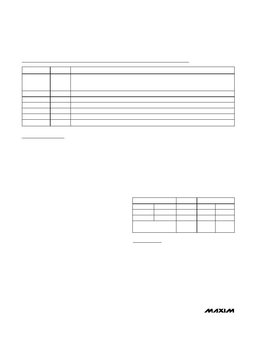
Pin Description
PIN
NAME
FUNCTION
1EN
Driver Enable Input. The driver is disabled when EN is low. EN is internally pulled down. When EN =
high and
EN = low or open, the outputs are active. For other combinations of EN and EN, the
outputs are disabled and are high impedance.
2, 3, 6, 7
IN_
LVTTL/LVCMOS Driver Inputs
4VCC
Power-Supply Input. Bypass VCC to GND with 0.1F and 0.001F ceramic capacitors.
5
GND
Ground
8
EN
Driver Enable Input. The transmitter is disabled when
EN is high. EN is internally pulled down.
9, 12, 13, 16
OUT_-
Inverting LVDS Driver Outputs
10, 11, 14, 15
OUT_+
Noninverting LVDS Driver Outputs
Detailed Description
The LVDS interface standard is a signaling method
intended for point-to-point communication over a con-
trolled-impedance medium as defined by the
ANSI/TIA/EIA-644 and IEEE 1596.3 standards. The
LVDS standard uses a lower voltage swing than other
common communication standards, achieving higher
data rates with reduced power consumption while
reducing EMI emissions and system susceptibility to
noise.
The MAX9123 is an 800Mbps quad differential LVDS
driver that is designed for high-speed, point-to-point,
and low-power applications. This device accepts
LVTTL/LVCMOS input levels and translates them to
LVDS output signals.
The MAX9123 generates a 2.5mA to 4.0mA output cur-
rent using a current-steering configuration. This current-
steering approach induces less ground bounce and no
shoot-through current, enhancing noise margin and sys-
tem speed performance. The driver outputs are short-
circuit current limited, and enter a high-impedance state
when the device is not powered or is disabled.
The current-steering architecture of the MAX9123
requires a resistive load to terminate the signal and
complete the transmission loop. Because the device
switches current and not voltage, the actual output volt-
age swing is determined by the value of the termination
resistor at the input of an LVDS receiver. Logic states
are determined by the direction of current flow through
the termination resistor. With a typical 3.7mA output
current, the MAX9123 produces an output voltage of
370mV when driving a 100
load.
Termination
Because the MAX9123 is a current-steering device, no
output voltage will be generated without a termination
resistor. The termination resistors should match the dif-
ferential impedance of the transmission line. Output
voltage levels depend upon the value of the termination
resistor. The MAX9123 is optimized for point-to-point
interface with 100
termination resistors at the receiver
inputs. Termination resistance values may range
between 90
and132, depending on the characteris-
tic impedance of the transmission medium.
Applications Information
Power-Supply Bypassing
Bypass VCC with high-frequency, surface-mount
ceramic 0.1F and 0.001F capacitors in parallel as
close to the device as possible, with the smaller valued
capacitor closest to VCC.
Differential Traces
Output trace characteristics affect the performance of
the MAX9123. Use controlled-impedance traces to
match trace impedance to the transmission medium.
ENABLES
INPUTS
OUTPUTS
EN
EN
IN_
OUT_+
OUT_ -
H
L or open
L
H
L or open
H
L
All other combinations
of ENABLE pins
Don’t
care
ZZ
Table 1. Input/Output Function Table
相關(guān)PDF資料 |
PDF描述 |
|---|---|
| VE-2WP-IW-F2 | CONVERTER MOD DC/DC 13.8V 100W |
| VI-JWL-MW-F4 | CONVERTER MOD DC/DC 28V 100W |
| VE-2WP-IW-F1 | CONVERTER MOD DC/DC 13.8V 100W |
| MAX9121EUE+ | IC RCVR QUAD LVDS 16-TSSOP |
| VI-JWL-MW-F3 | CONVERTER MOD DC/DC 28V 100W |
相關(guān)代理商/技術(shù)參數(shù) |
參數(shù)描述 |
|---|---|
| MAX9123EUE+ | 功能描述:LVDS 接口集成電路 Quad LVDS Line Driver RoHS:否 制造商:Texas Instruments 激勵器數(shù)量:4 接收機數(shù)量:4 數(shù)據(jù)速率:155.5 Mbps 工作電源電壓:5 V 最大功率耗散:1025 mW 最大工作溫度:+ 85 C 封裝 / 箱體:SOIC-16 Narrow 封裝:Reel |
| MAX9123EUE+G60 | 功能描述:LVDS 接口集成電路 Quad LVDS Line Transmitter with Flow-Through Pinout RoHS:否 制造商:Texas Instruments 激勵器數(shù)量:4 接收機數(shù)量:4 數(shù)據(jù)速率:155.5 Mbps 工作電源電壓:5 V 最大功率耗散:1025 mW 最大工作溫度:+ 85 C 封裝 / 箱體:SOIC-16 Narrow 封裝:Reel |
| MAX9123EUE+T | 功能描述:LVDS 接口集成電路 Quad LVDS Line Driver RoHS:否 制造商:Texas Instruments 激勵器數(shù)量:4 接收機數(shù)量:4 數(shù)據(jù)速率:155.5 Mbps 工作電源電壓:5 V 最大功率耗散:1025 mW 最大工作溫度:+ 85 C 封裝 / 箱體:SOIC-16 Narrow 封裝:Reel |
| MAX9123EUE+TG60 | 功能描述:LVDS 接口集成電路 Quad LVDS Line Driver with Flow-Through Pinout RoHS:否 制造商:Texas Instruments 激勵器數(shù)量:4 接收機數(shù)量:4 數(shù)據(jù)速率:155.5 Mbps 工作電源電壓:5 V 最大功率耗散:1025 mW 最大工作溫度:+ 85 C 封裝 / 箱體:SOIC-16 Narrow 封裝:Reel |
| MAX9123EUE-T | 功能描述:LVDS 接口集成電路 RoHS:否 制造商:Texas Instruments 激勵器數(shù)量:4 接收機數(shù)量:4 數(shù)據(jù)速率:155.5 Mbps 工作電源電壓:5 V 最大功率耗散:1025 mW 最大工作溫度:+ 85 C 封裝 / 箱體:SOIC-16 Narrow 封裝:Reel |
發(fā)布緊急采購,3分鐘左右您將得到回復(fù)。