- 您現(xiàn)在的位置:買賣IC網(wǎng) > PDF目錄383540 > MAX9163ESA (MAXIM INTEGRATED PRODUCTS INC) Bus LVDS 3.3V Single Transceiver PDF資料下載
參數(shù)資料
| 型號(hào): | MAX9163ESA |
| 廠商: | MAXIM INTEGRATED PRODUCTS INC |
| 元件分類: | 通用總線功能 |
| 英文描述: | Bus LVDS 3.3V Single Transceiver |
| 中文描述: | LINE TRANSCEIVER, PDSO8 |
| 封裝: | 0.150 INCH, MS-012AA, SOIC-8 |
| 文件頁(yè)數(shù): | 8/11頁(yè) |
| 文件大?。?/td> | 206K |
| 代理商: | MAX9163ESA |
Detailed Description
The MAX9163 high-speed BLVDS transceiver is
designed specifically for heavily loaded multipoint bus
applications. The MAX9163 operates from a single 3.3V
power supply, and is pin compatible with DS92LV010A.
The transceiver consists of one differential BLVDS line
driver and one LVDS receiver. The driver outputs and
receiver inputs are connected internally to minimize
bus loading. The driver and receiver can be enabled or
disabled individually or simultaneously by the use of
enable logic inputs (DE,
RE
).
The MAX9163 driver output uses a current-steering
configuration to generate a 9mA (typ) output current.
This current-steering approach induces less ground
bounce and no shoot-through current, enhancing noise
margin and system speed performance. The outputs
are short-circuit current limited. The MAX9163 current-
steering output requires a resistive load to terminate the
signal and complete the transmission loop. With a typi-
cal 9mA output current, the MAX9163 produces a
243mV output voltage when driving a bus terminated
with two 54
resistors (9mA x 27
= 243mV).
The MAX9163 receiver detects a differential input as
low as 100mV and translates it to a single-ended out-
put. The device features an in-path fail-safe circuit that
sets the receiver output high when the receiver inputs
are undriven and open, terminated, or shorted.
Receiver In-Path Fail-Safe
The MAX9163 has in-path fail-safe circuitry, which is
designed with a +35mV input offset voltage, a 2.5μA
current source between V
CC
and the noninverting
input, and a 5μA current sink between the inverting
input and ground (
Figure 6). If the differential input is
open, the 2.5μA current source pulls the input to about
V
CC
- 0.7V and the 5μA source sink pulls the inverting
input to ground, which drives the receiver output high.
If the differential input is shorted or terminated with a
typical value termination resistor, the +35mV offset dri-
ves the receiver output high. If the input is terminated
and floating, the receiver output is driven high by the
+35mV offset, and the 2:1 current sink to current
source ratio (5μA:2.5μA) pulls the inputs to ground.
This can be an advantage when switching between dri-
vers on a multipoint bus. The change in common-mode
voltage on the MAX9163 is from ground to the typical
driver offset voltage of 1.2V. This is less than the
change from V
CC
to 1.2V found on some circuits where
the fail-safe circuitry pulls the bus to V
CC
.
Effects of Capacitive Loading
The characteristic impedance of a differential PC board
trace is uniformly reduced when equal capacitive loads
are attached at equal intervals (provided that the transi-
tion time of the signal being driven on the trace is
longer than the delay between loads). This kind of load-
ing is typical of multipoint buses where cards are
attached at 1in or 0.8in intervals along the length of a
backplane. The reduction in characteristic impedance
is approximated by the following formula:
where:
Z
DF-unloaded
= unloaded differential characteristic
impedance
C
O
= unloaded trace capacitance (pF/unit length)
C
L
= value of each capacitive load (pF)
N = number of capacitive loads
L = trace length
Z
Z
x
C
[
C
N x C
(
L
DF loaded
DF unloaded
O
O
L
=
+
/ (
/ ))]
M
Bus LVDS 3.3V Single Transceiver
8
_______________________________________________________________________________________
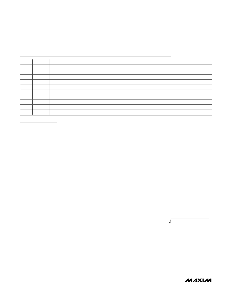
Pin Description
PIN
NAME
FUNCTION
1
DE
LVTTL/LVCMOS Driver Enable Input. The driver is enabled when DE is high. When DE is low, the driver output
is disabled and is high impedance.
LVTTL/LVCMOS Driver Input
LVTTL/LVCMOS Receiver Output
Ground
LVTTL/LVCMOS Receiver Enable Input. The receiver is enabled when
RE
is low. When
RE
is high, the receiver
output is disabled and is high impedance.
Inverting BLVDS Driver Output/Receiver Input
Noninverting BLVDS Driver Output/Receiver Input
Power-Supply Input. Bypass V
CC
to GND with 0.1μF and 0.001μF ceramic capacitors.
2
3
4
DIN
ROUT
GND
5
RE
6
7
8
DO-/RI-
DO+/RI+
V
CC
相關(guān)PDF資料 |
PDF描述 |
|---|---|
| MAX9163 | Bus LVDS 3.3V Single Transceiver |
| MAX9169-MAX9170 | 4-Port LVDS and LVTTL-to-LVDS Repeaters |
| MAX9169ESE | 4-Port LVDS and LVTTL-to-LVDS Repeaters |
| MAX9169EUE | 4-Port LVDS and LVTTL-to-LVDS Repeaters |
| MAX9170ESE | 4-Port LVDS and LVTTL-to-LVDS Repeaters |
相關(guān)代理商/技術(shù)參數(shù) |
參數(shù)描述 |
|---|---|
| MAX9163ESA+ | 功能描述:LVDS 接口集成電路 Bus LVDS 3.3V Single Transceiver RoHS:否 制造商:Texas Instruments 激勵(lì)器數(shù)量:4 接收機(jī)數(shù)量:4 數(shù)據(jù)速率:155.5 Mbps 工作電源電壓:5 V 最大功率耗散:1025 mW 最大工作溫度:+ 85 C 封裝 / 箱體:SOIC-16 Narrow 封裝:Reel |
| MAX9163ESA+T | 功能描述:LVDS 接口集成電路 Bus LVDS 3.3V Single Transceiver RoHS:否 制造商:Texas Instruments 激勵(lì)器數(shù)量:4 接收機(jī)數(shù)量:4 數(shù)據(jù)速率:155.5 Mbps 工作電源電壓:5 V 最大功率耗散:1025 mW 最大工作溫度:+ 85 C 封裝 / 箱體:SOIC-16 Narrow 封裝:Reel |
| MAX9163ESA-T | 功能描述:LVDS 接口集成電路 Bus LVDS 3.3V Single Transceiver RoHS:否 制造商:Texas Instruments 激勵(lì)器數(shù)量:4 接收機(jī)數(shù)量:4 數(shù)據(jù)速率:155.5 Mbps 工作電源電壓:5 V 最大功率耗散:1025 mW 最大工作溫度:+ 85 C 封裝 / 箱體:SOIC-16 Narrow 封裝:Reel |
| MAX9164 | 制造商:MAXIM 制造商全稱:Maxim Integrated Products 功能描述:3.3V Single LVDS Driver/Receiver |
| MAX9164ESD | 制造商:Maxim Integrated Products 功能描述: 制造商:Maxim Integrated Products 功能描述:3.3V SINGLE LVDS DRIVER/RECEIVER - Rail/Tube |
發(fā)布緊急采購(gòu),3分鐘左右您將得到回復(fù)。