- 您現(xiàn)在的位置:買賣IC網(wǎng) > PDF目錄383540 > MAX9172ESA (MAXIM INTEGRATED PRODUCTS INC) Single/Dual LVDS Line Receivers with “In-Path” Fail-Safe PDF資料下載
參數(shù)資料
| 型號: | MAX9172ESA |
| 廠商: | MAXIM INTEGRATED PRODUCTS INC |
| 元件分類: | 通用總線功能 |
| 英文描述: | Single/Dual LVDS Line Receivers with “In-Path” Fail-Safe |
| 中文描述: | DUAL LINE RECEIVER, PDSO8 |
| 封裝: | 0.150 INCH, MS-012AA, SOIC-8 |
| 文件頁數(shù): | 6/12頁 |
| 文件大小: | 303K |
| 代理商: | MAX9172ESA |
M
Detailed Description
LVDS Inputs
The MAX9171/MAX9172 feature LVDS inputs for inter-
facing high-speed digital circuitry. The LVDS interface
standard is a signaling method intended for point-to-
point communication over controlled-impedance
media, as defined by the ANSI TIA/EIA-644 standards.
The technology uses low-voltage signals to achieve fast
transition times and minimize power dissipation and
noise immunity. The MAX9171/MAX9172 convert LVDS
Table 1. Input-Output Function Table
signals to LVCMOS/LVTTL signals at rates in excess of
500Mbps. These devices are capable of detecting dif-
ferential signals as low as 100mV and as high as 1.2V
within a 0 to V
CC
input voltage range. Table 1 is the
input-output function table.
Fail-Safe
The MAX9171/MAX9172 fail-safe drives the receiver
output high when the differential input is:
Open
Undriven and shorted
Undriven and terminated
Without fail-safe, differential noise at the input may
switch the receiver and appear as data to the receiving
system. An open input occurs when a cable and termi-
nation are disconnected. An undriven, terminated input
occurs when a cable is disconnected with the termina-
tion still connected across the receiver inputs or when
the driver of a receiver is in high impedance. An undriv-
en, shorted input can occur due to a shorted cable.
Single/Dual LVDS Line Receivers with
“In-Path” Fail-Safe
6
_______________________________________________________________________________________
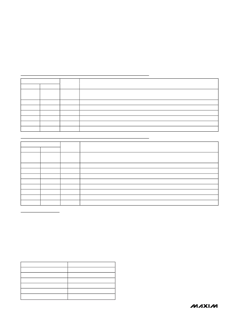
MAX9171 Pin Description
PIN
SOT23
SO/TDFN
NAME
FUNCTION
1
8
V
CC
Positive Power-Supply Input. Bypass with a 0.1μF and a 0.001μF capacitor to GND with the
smallest capacitor closest to the pin.
2
3
5
7
GND
OUT
N.C.
IN+
IN-
EP
Ground
Receiver Output
No Connection. Not internally connected.
Noninverting Differential Receiver Input
Inverting Differential Receiver Input
Exposed Paddle. Solder to PCB ground.
4, 5, 6
7
8
—
3, 4, 6
2
1
( TD FN onl y)
MAX9172 Pin Description
PIN
SOT23
SO/TDFN
NAME
FUNCTION
1
8
V
CC
Positive Power-Supply Input. Bypass with a 0.1μF and a 0.001μF capacitor to GND with the
smallest capacitor closest to the pin.
2
3
4
5
6
7
8
—
5
7
6
4
3
2
1
GND
OUT1
OUT2
IN2-
IN2+
IN1+
IN1-
EP
Ground
Receiver Output 1
Receiver Output 2
Inverting Differential Receiver Input 2
Noninverting Differential Receiver Input 2
Noninverting Differential Receiver Input 1
Inverting Differential Receiver Input 1
Exposed Paddle. Solder to PCB ground.
( TD FN onl y)
INPUTS
(IN_+) - (IN_-)
≥
0mV
≤
-100mV
Open
Undriven short
Undriven parallel termination
OUTPUT
OUT_
High
Low
High
High
High
相關(guān)PDF資料 |
PDF描述 |
|---|---|
| MAX9172ETA | Single/Dual LVDS Line Receivers with “In-Path” Fail-Safe |
| MAX9201EUE | Low-Cost, 7ns, Low-Power Voltage Comparators |
| MAX9202 | Low-Cost, 7ns, Low-Power Voltage Comparators |
| MAX9202ESD | Low-Cost, 7ns, Low-Power Voltage Comparators |
| MAX9202EUD | Low-Cost, 7ns, Low-Power Voltage Comparators |
相關(guān)代理商/技術(shù)參數(shù) |
參數(shù)描述 |
|---|---|
| MAX9172ESA+ | 制造商:Maxim Integrated Products 功能描述:LINE RCVR 2RX 8SOIC N - Rail/Tube |
| MAX9172ESA+T | 制造商:Maxim Integrated Products 功能描述:LINE RCVR 2RX 8SOIC N - Tape and Reel |
| MAX9172ESA-T | 制造商:Maxim Integrated Products 功能描述:SINGLE/DUAL LVDS LINE RECEIVERS WITH IN-PATH" - Tape and Reel |
| MAX9172ETA | 制造商:MAXIM 制造商全稱:Maxim Integrated Products 功能描述:Single/Dual LVDS Line Receivers with “In-Path” Fail-Safe |
| MAX9173 | 制造商:MAXIM 制造商全稱:Maxim Integrated Products 功能描述:Quad LVDS Line Receiver with Flow-Through Pinout and 揑n-Path?Fail-Safe |
發(fā)布緊急采購,3分鐘左右您將得到回復(fù)。