- 您現(xiàn)在的位置:買賣IC網(wǎng) > PDF目錄383540 > MAX9172ESA (MAXIM INTEGRATED PRODUCTS INC) Single/Dual LVDS Line Receivers with “In-Path” Fail-Safe PDF資料下載
參數(shù)資料
| 型號(hào): | MAX9172ESA |
| 廠商: | MAXIM INTEGRATED PRODUCTS INC |
| 元件分類: | 通用總線功能 |
| 英文描述: | Single/Dual LVDS Line Receivers with “In-Path” Fail-Safe |
| 中文描述: | DUAL LINE RECEIVER, PDSO8 |
| 封裝: | 0.150 INCH, MS-012AA, SOIC-8 |
| 文件頁數(shù): | 7/12頁 |
| 文件大小: | 303K |
| 代理商: | MAX9172ESA |
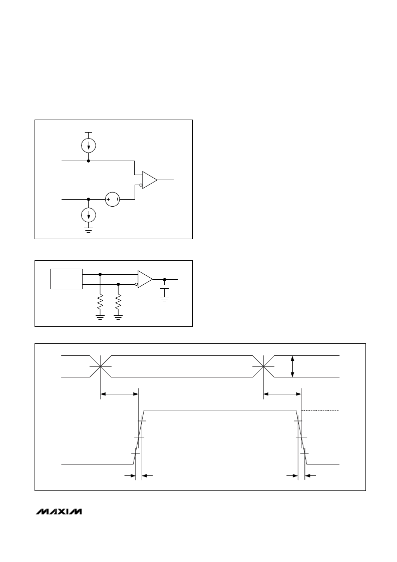
In-Path vs. Parallel Fail-Safe
The MAX9171/MAX9172 have in-path fail-safe that is
compatible with in-path fail-safe receivers, such as the
DS90LV018A and DS90LV028A. Refer to the MAX9111/
MAX9113 data sheet for pin-compatible receivers with
parallel fail-safe and lower jitter. Refer to the MAX9130
data sheet for a single LVDS receiver with parallel fail-
safe in an SC70 package.
The MAX9171/MAX9172 with in-path fail-safe are
designed with a +40mV input offset voltage, a 2.5μA
current source between V
CC
and the noninverting
input, and a 5μA current sink between the inverting
input and ground (Figure 1). If the differential input is
open, the 2.5μA current source pulls the input to V
CC
-
0.7V and the 5μA source sink pulls the inverting input to
ground, which drives the receiver output high. If the dif-
ferential input is shorted or terminated with a typical
value termination resistor, the +40mV offset drives the
receiver output high. If the input is terminated and float-
ing, the receiver output is driven high by the +40mV off-
set, and the 2:1 current sink to current source ratio
(5μA:2.5μA) pulls the inputs to ground. This can be an
advantage when switching between drivers on a multi-
point bus because the change in common-mode volt-
age from ground to the typical driver offset voltage of
1.2V is not as much as the change from V
CC
to 1.2V
(parallel fail-safe pulls the bus to V
CC
). Figure 2 shows
the propagation delay and transition test time circuit
and Figure 3 shows the propagation delay and transi-
tion test time waveforms.
M
Single/Dual LVDS Line Receivers with
“In-Path” Fail-Safe
_______________________________________________________________________________________
7
OUT_
V
CC
IN_+
IN_-
5
μ
A
2.5
μ
A
40mV
Figure 1. Input with In-Path Fail-Safe Network Equivalent Circuit
50
50
IN_-
OUT_
IN_+
15pF
PULSE
GENERATOR
Figure 2. Propagation Delay and Transition Test Time Circuit
IN_+
IN_-
t
PLHD
20%
80%
OUT_
V
OH
V
OL
1.5V
1.5V
20%
80%
1.2V (0V DIFFERENTIAL)
V
ID
= 0.2V
1.3V
1.1V
t
PHLD
t
THL
t
TLH
Figure 3. Propagation Delay and Transition Time Waveforms
相關(guān)PDF資料 |
PDF描述 |
|---|---|
| MAX9172ETA | Single/Dual LVDS Line Receivers with “In-Path” Fail-Safe |
| MAX9201EUE | Low-Cost, 7ns, Low-Power Voltage Comparators |
| MAX9202 | Low-Cost, 7ns, Low-Power Voltage Comparators |
| MAX9202ESD | Low-Cost, 7ns, Low-Power Voltage Comparators |
| MAX9202EUD | Low-Cost, 7ns, Low-Power Voltage Comparators |
相關(guān)代理商/技術(shù)參數(shù) |
參數(shù)描述 |
|---|---|
| MAX9172ESA+ | 制造商:Maxim Integrated Products 功能描述:LINE RCVR 2RX 8SOIC N - Rail/Tube |
| MAX9172ESA+T | 制造商:Maxim Integrated Products 功能描述:LINE RCVR 2RX 8SOIC N - Tape and Reel |
| MAX9172ESA-T | 制造商:Maxim Integrated Products 功能描述:SINGLE/DUAL LVDS LINE RECEIVERS WITH IN-PATH" - Tape and Reel |
| MAX9172ETA | 制造商:MAXIM 制造商全稱:Maxim Integrated Products 功能描述:Single/Dual LVDS Line Receivers with “In-Path” Fail-Safe |
| MAX9173 | 制造商:MAXIM 制造商全稱:Maxim Integrated Products 功能描述:Quad LVDS Line Receiver with Flow-Through Pinout and 揑n-Path?Fail-Safe |
發(fā)布緊急采購,3分鐘左右您將得到回復(fù)。