- 您現(xiàn)在的位置:買賣IC網(wǎng) > PDF目錄385555 > MAX9316 (Maxim Integrated Products, Inc.) Quadruple 2-Input Positive-NAND Gates 14-CFP -55 to 125 PDF資料下載
參數(shù)資料
| 型號: | MAX9316 |
| 廠商: | Maxim Integrated Products, Inc. |
| 英文描述: | Quadruple 2-Input Positive-NAND Gates 14-CFP -55 to 125 |
| 中文描述: | 1:5差分LVPECL/LVECL/HSTL時(shí)鐘和數(shù)據(jù)驅(qū)動(dòng)器 |
| 文件頁數(shù): | 6/12頁 |
| 文件大小: | 214K |
| 代理商: | MAX9316 |
M
Detailed Description
The MAX9316 is a low-skew, 1-to-5 differential driver
designed for clock or data distribution. A 2-to-1 MUX
selects one of the two clock inputs, CLK,
CLK
and
SCLK. The CLK and
CLK
input is differential while the
SCLK is single ended. The MUX is switched by the sin-
gle-ended SEL input. A logic low selects the CLK input
and a logic high selects the SCLK input. The SEL logic
threshold is set by the internal voltage reference V
BB
.
SEL input can be driven by V
CC
and V
EE
or by a single-
ended LVPECL/LVECL signal. The selected input is
reproduced at five differential outputs, Q0 to Q4.
Synchronous Enable
The MAX9316 is synchronously enabled and disabled
with outputs in the low state to eliminate shortened
clock pulses.
EN
is connected to the input of an edge-
triggered D flip-flop. After power-up, drive
EN
low and
toggle the selected clock input to enable the outputs.
The outputs are enabled on the falling edge of the
selected clock input after
EN
goes low. The outputs are
disabled to a low state on the falling edge of the select-
ed clock input after
EN
goes high. The threshold for
EN
is equal to V
BB
.
Supply
For interfacing to differential HSTL and LVPECL signals,
the V
CC
range is from +3.0 to +3.8V (with V
EE
ground-
1:5 Differential LVPECL/LVECL/HSTL
Clock and Data Driver
6
_______________________________________________________________________________________
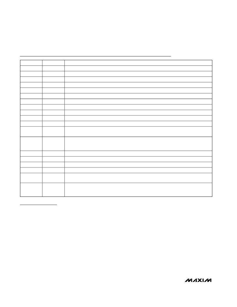
Pin Description
PIN
NAME
FUNCTION
1
Q0
Noninverting Q0 Output. Typically terminate with 50
resistor to (V
CC
- 2V).
Inverting Q0 Output. Typically terminate with 50
resistor to (V
CC
- 2V).
Noninverting Q1 Output. Typically terminate with 50
resistor to (V
CC
- 2V).
Inverting Q1 Output. Typically terminate with 50
resistor to (V
CC
- 2V).
Noninverting Q2 Output. Typically terminate with 50
resistor to (V
CC
- 2V).
Inverting Q2 Output. Typically terminate with 50
resistor to (V
CC
- 2V).
Noninverting Q3 Output. Typically terminate with 50
resistor to (V
CC
- 2V).
Inverting Q3 Output. Typically terminate with 50
resistor to (V
CC
- 2V).
Noninverting Q4 Output. Typically terminate with 50
resistor to (V
CC
- 2V).
Inverting Q4 Output. Typically terminate with 50
resistor to (V
CC
- 2V).
Negative Supply Voltage
2
Q0
3
Q1
4
Q1
5
Q2
6
Q2
7
Q3
8
Q3
9
Q4
10
Q4
11
V
EE
12
SEL
Clock Select Input (Single Ended). Drive low to select the CLK,
CLK
input. Drive high to select the
SCLK input. The SEL threshold is equal to V
BB
. Internal 60k
pulldown to V
EE
.
13
V
BB
Reference Output Voltage. Connect to the inverting or noninverting clock input to provide a
reference for single-ended operation. When used, bypass with a 0.01μF ceramic capacitor to V
CC
;
otherwise, leave it unconnected.
14
CLK
Inverting Differential Clock Input. Internal 75k
pullup to V
CC
and 75k
pulldown to V
EE
.
Noninverting Differential Clock Input. Internal 75k
pulldown to V
EE
.
Single-Ended Clock Input. Internal 75k
pulldown to V
EE
.
Not Internally Connected. Solder to PC board for package thermal dissipation.
15
CLK
16
SCLK
17
NC
18, 20
V
CC
Positive Supply Voltage. Bypass V
CC
to V
EE
with 0.1μF and 0.01μF ceramic capacitors. Place the
capacitors as close to the device as possible with the smaller value capacitor closest to the device.
19
EN
Output Enable Input. Outputs are synchronously enabled on the falling edge of the clock input
when
EN
is low. Outputs are synchronously set to low on the falling edge of the clock input when
EN
is high. Internal 60k
pulldown to V
EE
.
相關(guān)PDF資料 |
PDF描述 |
|---|---|
| MAX9316EUP | 1:5 Differential LVPECL/LVECL/HSTL Clock and Data Driver |
| MAX9320B | 1:2 Differential PECL/ECL/LVPECL/LVECL Clock and Data Driver |
| MAX9320BESA | 1:2 Differential PECL/ECL/LVPECL/LVECL Clock and Data Driver |
| MAX9320BEUA | 1:2 Differential PECL/ECL/LVPECL/LVECL Clock and Data Driver |
| MAX9392ETJ | Anything-to-LVDS Dual 2 x 2 Crosspoint Switches |
相關(guān)代理商/技術(shù)參數(shù) |
參數(shù)描述 |
|---|---|
| MAX9316AEWP | 功能描述:時(shí)鐘驅(qū)動(dòng)器及分配 RoHS:否 制造商:Micrel 乘法/除法因子:1:4 輸出類型:Differential 最大輸出頻率:4.2 GHz 電源電壓-最大: 電源電壓-最小:5 V 最大工作溫度:+ 85 C 封裝 / 箱體:SOIC-8 封裝:Reel |
| MAX9316AEWP-T | 功能描述:時(shí)鐘驅(qū)動(dòng)器及分配 RoHS:否 制造商:Micrel 乘法/除法因子:1:4 輸出類型:Differential 最大輸出頻率:4.2 GHz 電源電壓-最大: 電源電壓-最小:5 V 最大工作溫度:+ 85 C 封裝 / 箱體:SOIC-8 封裝:Reel |
| MAX9316EUP | 制造商:Maxim Integrated Products 功能描述:1:5 DIFFERENTIAL LVPECL/LVECL/HSTL CLOCK AND - Rail/Tube |
| MAX9316EUP+ | 功能描述:時(shí)鐘驅(qū)動(dòng)器及分配 RoHS:否 制造商:Micrel 乘法/除法因子:1:4 輸出類型:Differential 最大輸出頻率:4.2 GHz 電源電壓-最大: 電源電壓-最小:5 V 最大工作溫度:+ 85 C 封裝 / 箱體:SOIC-8 封裝:Reel |
| MAX9316EUP+T | 功能描述:時(shí)鐘驅(qū)動(dòng)器及分配 RoHS:否 制造商:Micrel 乘法/除法因子:1:4 輸出類型:Differential 最大輸出頻率:4.2 GHz 電源電壓-最大: 電源電壓-最小:5 V 最大工作溫度:+ 85 C 封裝 / 箱體:SOIC-8 封裝:Reel |
發(fā)布緊急采購,3分鐘左右您將得到回復(fù)。