- 您現(xiàn)在的位置:買賣IC網(wǎng) > PDF目錄385555 > MAX9320B (Maxim Integrated Products, Inc.) 1:2 Differential PECL/ECL/LVPECL/LVECL Clock and Data Driver PDF資料下載
參數(shù)資料
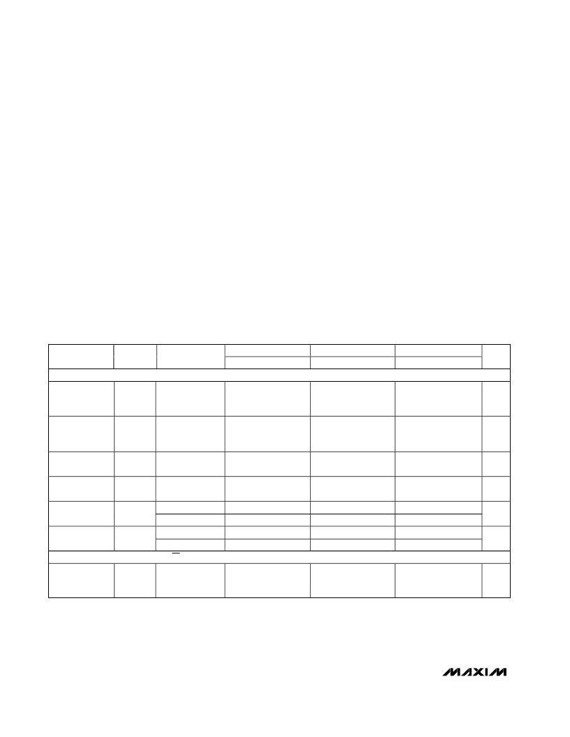
| 型號: | MAX9320B |
| 廠商: | Maxim Integrated Products, Inc. |
| 英文描述: | 1:2 Differential PECL/ECL/LVPECL/LVECL Clock and Data Driver |
| 中文描述: | 1:2差分PECL/ECL/LVPECL/LVECL時鐘和數(shù)據(jù)驅(qū)動器 |
| 文件頁數(shù): | 2/7頁 |
| 文件大小: | 120K |
| 代理商: | MAX9320B |
M
1:2 Differential PECL/ECL/LVPECL/LVECL
Clock and Data Driver
2
_______________________________________________________________________________________
ABSOLUTE MAXIMUM RATINGS
V
CC
to V
EE
.............................................................................+6V
D or
D
....................................................V
EE
- 0.3V to V
CC
+ 0.3V
D or
D
with the Other Floating............. V
CC
- 5.0V to V
CC
+ 0.3V
D to
D
.................................................................................±3.0V
Continuous Output Current.................................................50mA
Surge Output Current........................................................100mA
Continuous Output Power Dissipation (TA= +70°C)
8-Pin TSSOP
(derate 4.5mW/°C above +70°C).................................362mW
8-Pin SO
(derate 5.9mW/°C above +70°C).................................471mW
Junction-to-Ambient Thermal Resistance in Still Air
8-Pin TSSOP ............................................................+221°C/W
8-Pin SO...................................................................+170°C/W
DC ELECTRICAL CHARACTERISTICS
(V
CC
- V
EE
= 3.0V to 5.5V, outputs loaded with 50
±1% to V
CC
- 2V. Typical values are at V
CC
- V
EE
= 5.0V, V
IHD
= V
CC
- 1.0V, V
ILD
= V
CC
- 1.5V, unless otherwise noted.) (Notes 1, 2, 3)
Stresses beyond those listed under “Absolute Maximum Ratings” may cause permanent damage to the device. These are stress ratings only, and functional
operation of the device at these or any other conditions beyond those indicated in the operational sections of the specifications is not implied. Exposure to
absolute maximum rating conditions for extended periods may affect device reliability.
Junction-to-Ambient Thermal Resistance with 500
LFPM Airflow
8-Pin TSSOP ............................................................+155°C/W
8-Pin SO.....................................................................+99°C/W
Junction-to-Case Thermal Resistance
8-Pin TSSOP ..............................................................+39°C/W
8-Pin SO.....................................................................+40°C/W
Operating Temperature Range ...........................-40°C to +85°C
Junction Temperature......................................................+150°C
Storage Temperature Range.............................-65°C to +150°C
ESD Protection
Human Body Model (D,
D
, Q_,
Q_
) .................................>2kV
Soldering Temperature (10s)...........................................+300°C
-40
°
C
TYP
+25
°
C
TYP
+85
°
C
TYP
PARAMETER
SYM BOL
CONDITIONS
MIN
MAX
MIN
MAX
MIN
MAX
UNITS
DIFFERENTIAL INPUT (D,
D
)
High Voltage of
Differential
Input
V
IHD
V
EE
+ 1.2
V
CC
V
EE
+ 1.2
V
CC
V
EE
+ 1.2
V
CC
V
Low Voltage of
Differential
Input
V
ILD
V
EE
V
CC
- 0.1
V
EE
V
CC
- 0.1
V
EE
V
CC
- 0.1
V
Differential
Input Voltage
V
IHD
-
V
ILD
0.1
3.0
0.1
3.0
0.1
3.0
V
Input High
Current
I
IH
150
150
150
μA
V
CC
- V
EE
≤
3.8V
V
CC
- V
EE
≥
3.8V
V
CC
- V
EE
≤
3.8V
V
CC
- V
EE
≥
3.8V
-100
-140
-150
-175
+100
+140
+150
+175
-100
-150
-175
+100
+140
+150
+175
-100
-140
-150
-175
+100
+140
+150
+175
D Input Low
Current
I
ILD
μA
D
Input Low
Current
I
IL
D
μA
DIFFERENTIAL OUTPUTS (Q_,
Q__
)
Single-Ended
Output High
Voltage
V
OH
Figure 1
V
CC
- 1.135
V
CC
- 0.885
V
CC
- 1.07
V
CC
- 0.82
V
CC
- 1.01
V
CC
- 0.76
V
相關PDF資料 |
PDF描述 |
|---|---|
| MAX9320BESA | 1:2 Differential PECL/ECL/LVPECL/LVECL Clock and Data Driver |
| MAX9320BEUA | 1:2 Differential PECL/ECL/LVPECL/LVECL Clock and Data Driver |
| MAX9392ETJ | Anything-to-LVDS Dual 2 x 2 Crosspoint Switches |
| MAX9393ETJ | Anything-to-LVDS Dual 2 x 2 Crosspoint Switches |
| MAX9406 | DisplayPort to DVI/HDMI Level Shifter |
相關代理商/技術參數(shù) |
參數(shù)描述 |
|---|---|
| MAX9320BESA | 制造商:Rochester Electronics LLC 功能描述: 制造商:Maxim Integrated Products 功能描述: |
| MAX9320BESA+ | 制造商:Maxim Integrated Products 功能描述:LINE TRANSMITTER 1TX 8SOIC N - Rail/Tube |
| MAX9320BESA+T | 制造商:Maxim Integrated Products 功能描述:LINE TRANSMITTER 1TX 8SOIC N - Tape and Reel |
| MAX9320BESA-T | 制造商:Maxim Integrated Products 功能描述:1:2 DIFFERENTIAL PECL/ECL/LVPECL/LVECL CLOCK - Tape and Reel |
| MAX9320BEUA | 制造商:Maxim Integrated Products 功能描述:1:2 DIFFERENTIAL PECL/ECL/LVPECL/LVECL CLOCK - Rail/Tube |
發(fā)布緊急采購,3分鐘左右您將得到回復。