- 您現(xiàn)在的位置:買賣IC網(wǎng) > PDF目錄385555 > MAX9393ETJ (MAXIM INTEGRATED PRODUCTS INC) Anything-to-LVDS Dual 2 x 2 Crosspoint Switches PDF資料下載
參數(shù)資料
| 型號: | MAX9393ETJ |
| 廠商: | MAXIM INTEGRATED PRODUCTS INC |
| 元件分類: | 運動控制電子 |
| 英文描述: | Anything-to-LVDS Dual 2 x 2 Crosspoint Switches |
| 中文描述: | DUAL 2-CHANNEL, CROSS POINT SWITCH, QCC32 |
| 封裝: | 5 X 5 MM, 0.80 MM HEIGHT, TQFN-32 |
| 文件頁數(shù): | 1/14頁 |
| 文件大?。?/td> | 309K |
| 代理商: | MAX9393ETJ |
General Description
The MAX9392/MAX9393 dual 2 x 2 crosspoint switches
perform high-speed, low-power, and low-noise signal
distribution. The MAX9392/MAX9393 multiplex one of two
differential input pairs to either or both low-voltage differ-
ential signaling (LVDS) outputs for each channel.
Independent enable inputs turn on or turn off each differ-
ential output pair.
Four LVCMOS/LVTTL logic inputs (two per channel) con-
trol the internal connections between inputs and outputs.
This flexibility allows for the following configurations: 2 x 2
crosspoint switch, 2:1 mux, 1:2 splitter, or dual repeater.
This makes the MAX9392/MAX9393 ideal for protection
switching in fault-tolerant systems, loopback switching for
diagnostics, fanout buffering for clock/data distribution,
and signal regeneration.
Fail-safe circuitry forces the outputs to a differential low
condition for undriven inputs or when the common-
mode voltage exceeds the specified range. The
MAX9392 provides high-level input fail-safe detection
for LVDS, HSTL, and other GND-referenced differential
inputs. The MAX9393 provides low-level input fail-safe
detection for LVPECL, CML, and other V
CC
-referenced
differential inputs.
Ultra-low 98ps
(
P-P)
(max) pseudorandom bit sequence
(PRBS) jitter ensures reliable communications in high-
speed links that are highly sensitive to timing error,
especially those incorporating clock-and-data recovery,
or serializers and deserializers. The high-speed switch-
ing performance guarantees 1.5GHz operation and less
than 67ps (max) skew between channels.
LVDS inputs and outputs are compatible with the
TIA/EIA-644 LVDS standard. The LVDS outputs drive
100
loads. The MAX9392/MAX9393 are offered in
5mm x 5mm thin QFN with exposed paddle and 32-pin
TQFP packages and operate over the extended tem-
perature range (-40°C to +85°C).
Also see the MAX9390/MAX9391 for the crossflow version.
Applications
High-Speed Telecom/Datacom Equipment
Central-Office Backplane Clock Distribution
DSLAM
Protection Switching
Fault-Tolerant Systems
Features
o
1.5GHz Operation with 250mV Differential Output
Swing
o
2ps
RMS
(max) Random Jitter
o
AC Specifications Guaranteed for 150mV
Differential Input
o
Signal Inputs Accept Any Differential Signaling
Standard
o
LVDS Outputs for Clock or High-Speed Data
o
High-Level Input Fail-Safe Detection (MAX9392)
o
Low-Level Input Fail-Safe Detection (MAX9393)
o
+3.0V to +3.6V Supply Voltage Range
o
LVCMOS/LVTTL Logic Inputs Control Signal
Routing
M
Anything-to-LVDS Dual 2 x 2
Crosspoint Switches
________________________________________________________________
Maxim Integrated Products
For pricing, delivery, and ordering information, please contact Maxim/Dallas Direct! at
1-888-629-4642, or visit Maxim’s website at www.maxim-ic.com.
1
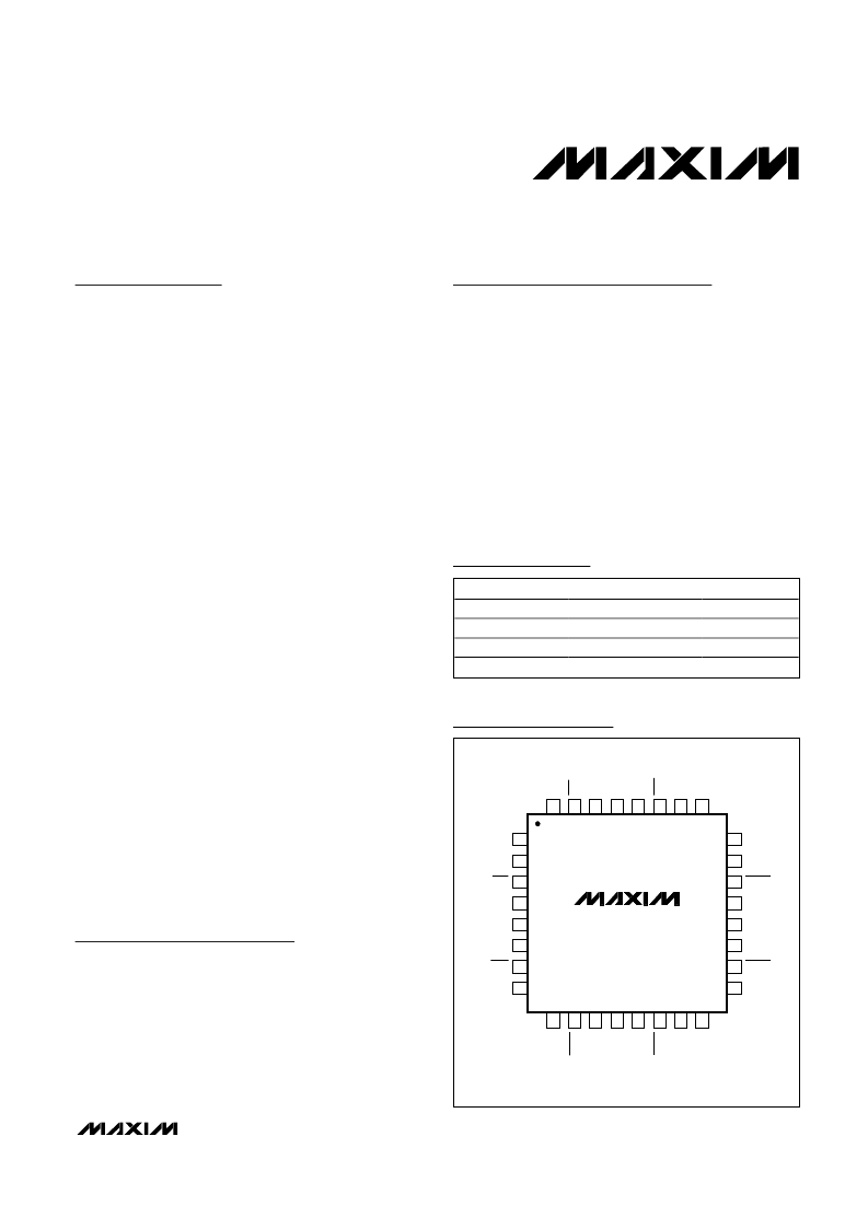
TOP VIEW
MAX9392
MAX9393
TQFP
32
28
29
30
31
25
26
27
I
I
V
C
A
A
I
I
G
10
O
13
E
15
O
14
O
16
V
C
11
O
12
G
9
E
17
18
19
20
21
22
23 OUTA0
24 V
CC
OUTA0
ENA0
GND
OUTA1
OUTA1
ENA1
2
3
4
5
6
7
8
BSEL1
INB1
INB1
BSEL0
INB0
INB0
1
GND
V
CC
PART
TEMP RANGE
-40
°
C to +85
°
C
-40
°
C to +85
°
C
-40
°
C to +85
°
C
-40
°
C to +85
°
C
PIN-PACKAGE
32 TQFP
32 Thin QFN
32 TQFP
32 Thin QFN
MAX9392
EHJ
MAX9392ETJ*
MAX9393
EHJ
MAX9393ETJ*
Pin Configurations
Ordering Information
19-2913; Rev 0; 8/03
*
Future product—contact factory for availability.
Pin Configurations continued at end of data sheet.
Functional Diagram and Typical Operating Circuit appear at
end of data sheet.
相關(guān)PDF資料 |
PDF描述 |
|---|---|
| MAX9406 | DisplayPort to DVI/HDMI Level Shifter |
| MAX941 | High-Speed, Low-Power, 3V/5V, Rail-to-Rail Single-Supply Comparators(3V和5V,75ns,滿量程輸入比較器) |
| MAX9450EHJ | High-Precision Clock Generators with Integrated VCXO |
| MAX9450_07 | High-Precision Clock Generators with Integrated VCXO |
| MAX9451EHJ | High-Precision Clock Generators with Integrated VCXO |
相關(guān)代理商/技術(shù)參數(shù) |
參數(shù)描述 |
|---|---|
| MAX9393ETJ+ | 功能描述:模擬和數(shù)字交叉點 IC Anything-to-LVDS Dual 2 x 2 Crosspoint Switches RoHS:否 制造商:Micrel 配置:2 x 2 封裝 / 箱體:MLF-16 數(shù)據(jù)速率:10.7 Gbps 輸入電平:CML, LVDS, LVPECL 輸出電平:CML 電源電壓-最大:3.6 V 電源電壓-最小:2.375 V 最大工作溫度:+ 85 C 最小工作溫度:- 40 C 產(chǎn)品:Digital Crosspoint 封裝:Tube |
| MAX9393ETJ+T | 功能描述:模擬和數(shù)字交叉點 IC RoHS:否 制造商:Micrel 配置:2 x 2 封裝 / 箱體:MLF-16 數(shù)據(jù)速率:10.7 Gbps 輸入電平:CML, LVDS, LVPECL 輸出電平:CML 電源電壓-最大:3.6 V 電源電壓-最小:2.375 V 最大工作溫度:+ 85 C 最小工作溫度:- 40 C 產(chǎn)品:Digital Crosspoint 封裝:Tube |
| MAX9393ETJ-T | 功能描述:模擬和數(shù)字交叉點 IC RoHS:否 制造商:Micrel 配置:2 x 2 封裝 / 箱體:MLF-16 數(shù)據(jù)速率:10.7 Gbps 輸入電平:CML, LVDS, LVPECL 輸出電平:CML 電源電壓-最大:3.6 V 電源電壓-最小:2.375 V 最大工作溫度:+ 85 C 最小工作溫度:- 40 C 產(chǎn)品:Digital Crosspoint 封裝:Tube |
| MAX9394EHJ | 制造商:Maxim Integrated Products 功能描述:- Rail/Tube |
| MAX9394EHJ+ | 制造商:Maxim Integrated Products 功能描述:LVDS SERDES 0.45V TQFP - Rail/Tube |
發(fā)布緊急采購,3分鐘左右您將得到回復(fù)。