- 您現(xiàn)在的位置:買(mǎi)賣(mài)IC網(wǎng) > PDF目錄385555 > MAX9452EHJ (MAXIM INTEGRATED PRODUCTS INC) High-Precision Clock Generators with Integrated VCXO PDF資料下載
參數(shù)資料
| 型號(hào): | MAX9452EHJ |
| 廠商: | MAXIM INTEGRATED PRODUCTS INC |
| 元件分類: | 時(shí)鐘及定時(shí) |
| 英文描述: | High-Precision Clock Generators with Integrated VCXO |
| 中文描述: | 9452 SERIES, PLL BASED CLOCK DRIVER, 2 TRUE OUTPUT(S), 0 INVERTED OUTPUT(S), PQFP32 |
| 封裝: | 5 X 5 MM, 1 MM HEIGHT, MS-026-AAA-HD, TQFP-32 |
| 文件頁(yè)數(shù): | 10/18頁(yè) |
| 文件大小: | 323K |
| 代理商: | MAX9452EHJ |
第1頁(yè)第2頁(yè)第3頁(yè)第4頁(yè)第5頁(yè)第6頁(yè)第7頁(yè)第8頁(yè)第9頁(yè)當(dāng)前第10頁(yè)第11頁(yè)第12頁(yè)第13頁(yè)第14頁(yè)第15頁(yè)第16頁(yè)第17頁(yè)第18頁(yè)
M
High-Precision Clock Generators
with Integrated VCXO
10
______________________________________________________________________________________
External Loop Filter
When the device switches from one input reference to
the other or reverts to an input reference from holdover,
the output phase changes smoothly during the transition
due to the narrowband external PLL filter. The narrower
the filter bandwidth is, the smoother the phase
transition. However, if bandwidth is too narrow, it can
cause some degradation on output jitter performance.
Charge-Pump Current Setting
The MAX9450/MAX9451/MAX9452 allow external setting
of the charge-pump current in the PLL. Connect a resis-
tor from RJ to GNDA to set the PLL charge-pump current:
charge-pump current (μA) = 2.48 x 1000 /
(R
SET
(k
Ω
) + 0.375)
where R
SET
is in k
Ω
and the value of the charge-pump
current is in μA. Use R
SET
to adjust the loop response
to meet individual application requirements. The
charge-pump current and the external filter compo-
nents change the PLL bandwidth. Table 11 shows the
charge-pump current vs. the resistor’s value.
The loop response equation is defined as:
unity-gain bandwidth = (I
CP
x R
FILT
x 12kHz) / M
where I
CP
is the charge-pump current set by REXT,
R
FILT
is the external filter resistance, and M is the feed-
back divider.
Input Disable
The two inputs can be disabled separately by SEL0
and SEL1 or the 2 bits in CR5[3:2]. Table 2 shows the
state map.
Power-Up and Master Reset
Upon power-up, default frequency divider rates and the
states of the monitor, inputs, and outputs are set
according to Table 10. Setting MR high or CR6[4] to 1
also resets the device. When the device resets, INT
and CR7[5:6] go low and all the registers revert to their
default values.
I
2
C Interface
The control interface of the MAX9450/MAX9451/MAX9452
is an I
2
C or SPI depending on the states of AD0 and
AD1. Drive both AD0 and AD1 high to active SPI mode.
Otherwise, I
2
C is activated. The device operates as a
slave that sends and receives data through the clock
line, SCL, and data line, SDA, to achieve bidirectional
communication with the masters. A master (typically a
microcontroller) initiates all data transfers to and from
slaves, and generates the SCL clock that synchronizes
the data transfer. Figure 4 shows the timing of SCL and
SDA. The SDA line operates as both an input and an
open-drain output. SDA requires a pullup resistor, typi-
cally 4.7k
Ω
. The SCL line operates only as an input. A
pullup resistor, typically 4.7k
Ω
, is required on SCL if there
are multiple masters on the 2-wire bus, or if the master in
a single-master system has an open-drain SCL output.
I
2
C Device Address
Every I
2
C port has a 7-bit device address. This 7-bit
address is the slave (MAX9450/MAX9451/MAX9452)
ID for the master to write and read. In the MAX9450/
MAX9451/MAX9452, the first 4 bits (1101) of the
address are hard coded into the device at the factory.
See Table 3. The last 3 bits of the address are input
programmable by the three-level AD0 and AD1. This
configuration provides eight selectable addresses for
the MAX9450/MAX9451/MAX9452, allowing eight
devices to be connected to one master.
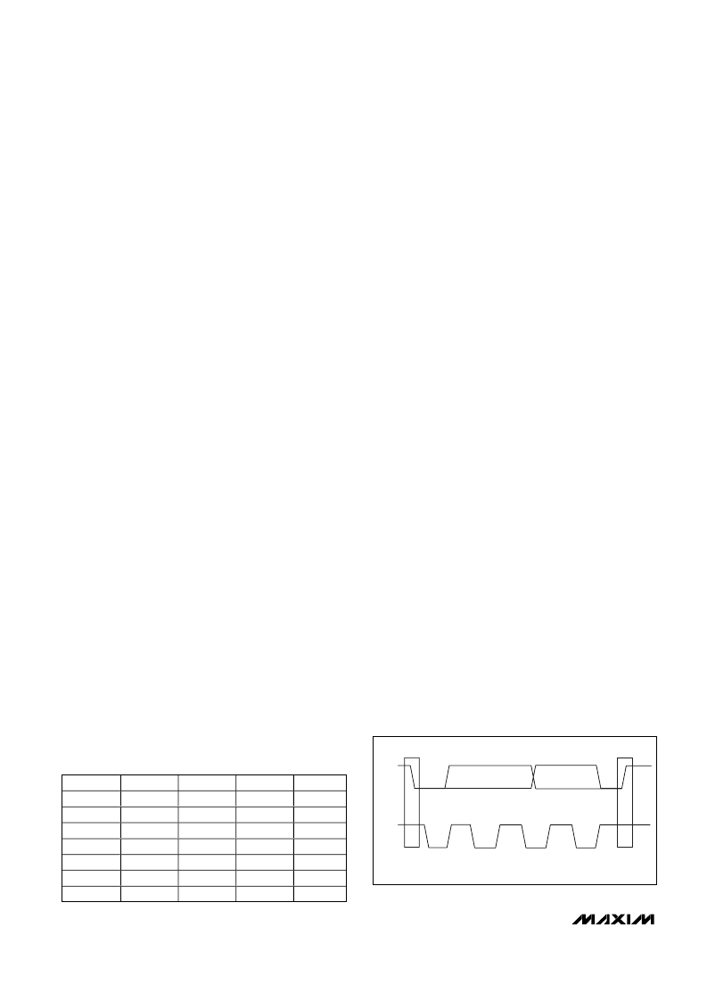
START and STOP Conditions
Both SCL and SDA remain high when the interface is
not busy. The active master signals the beginning of a
transmission with a START (S) condition by transitioning
SDA from high to low while SCL is high. When the master
has finished communicating with the slave, it issues a
STOP (P) condition by transitioning SDA from low to
high while SCL is high. The bus is then free for another
transmission (Figure 3). The interval between a START
and a STOP is called a session.
SEL1
0
0
1
1
X
X
X
SEL0
0
1
0
1
X
X
X
CR5[3:2]
00
00
00
00
01
10
11
IN1
IN0
Disabled
Disabled
Enabled
Enabled
Disabled
Enabled
Enabled
Disabled
Enabled
Disabled
Enabled
Enabled
Disabled
Enabled
Table 2. Input Activation by SEL0, SEL1,
or CR5[3:2]
SDA
SCL
S
START
CONDITION
P
STOP
CONDITION
Figure 3. START and STOP Conditions
相關(guān)PDF資料 |
PDF描述 |
|---|---|
| MAX9471 | Multiple-Output Clock Generators with Dual PLLs and OTP |
| MAX9471ETP | Multiple-Output Clock Generators with Dual PLLs and OTP |
| MAX9472 | Multiple-Output Clock Generators with Dual PLLs and OTP |
| MAX9472EUD | Multiple-Output Clock Generators with Dual PLLs and OTP |
| MAX9483 | Dual-Output, Multimode CD-RW/DVD Laser-Diode Drivers |
相關(guān)代理商/技術(shù)參數(shù) |
參數(shù)描述 |
|---|---|
| MAX9452EHJ+ | 功能描述:時(shí)鐘發(fā)生器及支持產(chǎn)品 High-Precision Clock Generator RoHS:否 制造商:Silicon Labs 類型:Clock Generators 最大輸入頻率:14.318 MHz 最大輸出頻率:166 MHz 輸出端數(shù)量:16 占空比 - 最大:55 % 工作電源電壓:3.3 V 工作電源電流:1 mA 最大工作溫度:+ 85 C 安裝風(fēng)格:SMD/SMT 封裝 / 箱體:QFN-56 |
| MAX9452EHJ+T | 功能描述:時(shí)鐘發(fā)生器及支持產(chǎn)品 High-Precision Clock Generator RoHS:否 制造商:Silicon Labs 類型:Clock Generators 最大輸入頻率:14.318 MHz 最大輸出頻率:166 MHz 輸出端數(shù)量:16 占空比 - 最大:55 % 工作電源電壓:3.3 V 工作電源電流:1 mA 最大工作溫度:+ 85 C 安裝風(fēng)格:SMD/SMT 封裝 / 箱體:QFN-56 |
| MAX9452EHJ-T | 功能描述:時(shí)鐘發(fā)生器及支持產(chǎn)品 High-Precision Clock Generator RoHS:否 制造商:Silicon Labs 類型:Clock Generators 最大輸入頻率:14.318 MHz 最大輸出頻率:166 MHz 輸出端數(shù)量:16 占空比 - 最大:55 % 工作電源電壓:3.3 V 工作電源電流:1 mA 最大工作溫度:+ 85 C 安裝風(fēng)格:SMD/SMT 封裝 / 箱體:QFN-56 |
| MAX9471ETP | 制造商:Maxim Integrated Products 功能描述:MULTIPLE OUTPUT CLOCK GENERATOR WIT - Rail/Tube |
| MAX9471ETP+ | 功能描述:時(shí)鐘發(fā)生器及支持產(chǎn)品 Multiple Output Clock Generator RoHS:否 制造商:Silicon Labs 類型:Clock Generators 最大輸入頻率:14.318 MHz 最大輸出頻率:166 MHz 輸出端數(shù)量:16 占空比 - 最大:55 % 工作電源電壓:3.3 V 工作電源電流:1 mA 最大工作溫度:+ 85 C 安裝風(fēng)格:SMD/SMT 封裝 / 箱體:QFN-56 |
發(fā)布緊急采購(gòu),3分鐘左右您將得到回復(fù)。