- 您現(xiàn)在的位置:買賣IC網(wǎng) > PDF目錄377883 > MB81116822A-84 (Fujitsu Limited) CMOS 2×1M ×8 BIT Hyper Page Mode Dynamic RAM(CMOS 2×1M ×8位超級頁面存取模式動態(tài)RAM) PDF資料下載
參數(shù)資料
| 型號: | MB81116822A-84 |
| 廠商: | Fujitsu Limited |
| 英文描述: | CMOS 2×1M ×8 BIT Hyper Page Mode Dynamic RAM(CMOS 2×1M ×8位超級頁面存取模式動態(tài)RAM) |
| 中文描述: | 的CMOS 2 × 100萬× 8位超頁模式動態(tài)RAM(2 × 100萬的CMOS × 8位超級頁面存取模式動態(tài)內(nèi)存) |
| 文件頁數(shù): | 19/43頁 |
| 文件大小: | 276K |
| 代理商: | MB81116822A-84 |
第1頁第2頁第3頁第4頁第5頁第6頁第7頁第8頁第9頁第10頁第11頁第12頁第13頁第14頁第15頁第16頁第17頁第18頁當(dāng)前第19頁第20頁第21頁第22頁第23頁第24頁第25頁第26頁第27頁第28頁第29頁第30頁第31頁第32頁第33頁第34頁第35頁第36頁第37頁第38頁第39頁第40頁第41頁第42頁第43頁

19
MB81116822A-125/-100/-84/-67
DATA INPUT AND OUTPUT (DQ
0
to DQ
7
)
Input data is latched and written into the memory at the clock following the Write command input. Data output
is obtained by the following conditions followed by a Read command input:
t
RAC
: from the Bank Active command when t
RCD
(min) is satisfied. (This parameter is reference only.)
t
CAC
: from the Read command when t
RCD
is greater than t
RCD
(min).
t
AC
: from the clock edge after t
RAC
and t
CAC
.
The polarity of the output data is identical to that of the input. Data is valid between access time (determined
by the three conditions above) and the next positive clock edge (t
OH
).
DATA I/O MASK (DQM)
DQM is an active high enable input and has an output disable and input mask function. During burst cycle and
when DQM = High is latched by a clock, input is masked at the same clock and output will be masked at the
second clock later while internal burst counter will increment by one or will go to the next stage depending on
burst type.
BURST MODE OPERATION AND BURST TYPE
The burst mode provides faster memory access. The burst mode is implemented by keeping the same Row
address and by automatic strobing column address. Access time and cycle time of Burst mode is specified as
t
AC
and t
CK
, respectively. The internal column address counter operation is determined by a mode register which
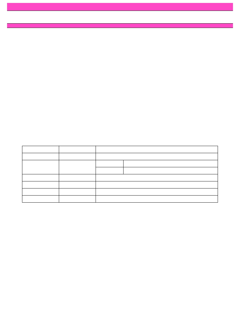
defines burst type and burst count length of 1,2 or 4 bits of boundary. In order to terminate or to move from the
current burst mode to the next stage while the remaining burst count is more than 1, the following combinations
will be required:
The burst type can be selected either sequential or interleave mode if burst length is 2 or 4. The sequential
mode is an incremental decoding scheme within a bundary address to be determined by count length, it
assigns+1 to the previous (or initial) address until reaching the end of boundary address and then wraps round
to least significant address(= 0). The interleave mode is a scrambled decoding scheme for A
0
and A
2
. If the first
access of column address is even (0), the next address will be odd (1), or vice-versa.
Current Stage
Next Stage
Method (Assert the following command)
Burst Read
Burst Read
Read Command
Burst Read
Burst Write
1st Step
Mask Command (Normally 3 clock cycles)
2nd Step
Write Command after l
OWD
Burst Write
Burst Write
Write Command
Burst Write
Burst Read
Read Command
Burst Read
Precharge
Precharge Command
Burst Write
Precharge
Precharge Command
相關(guān)PDF資料 |
PDF描述 |
|---|---|
| MB811171622A-100 | CMOS 2×512K×16 Bit Synchronous Dynamic RAM(CMOS 2×512K×16 位同步動態(tài)RAM) |
| MB811171622A-125 | CMOS 2×512K×16 Bit Synchronous Dynamic RAM(CMOS 2×512K×16 位同步動態(tài)RAM) |
| MB811171622A-67 | CMOS 2×512K×16 Bit Synchronous Dynamic RAM(CMOS 2×512K×16 位同步動態(tài)RAM) |
| MB811171622A-84 | CMOS 2×512K×16 Bit Synchronous Dynamic RAM(CMOS 2×512K×16 位同步動態(tài)RAM) |
| MB81117422A-100 | CMOS 2×2M ×4 Bit Synchronous Dynamic RAM(CMOS 2×2M ×4 位同步動態(tài)RAM) |
相關(guān)代理商/技術(shù)參數(shù) |
參數(shù)描述 |
|---|---|
| MB81141622-015PFTN | 制造商:FUJITSU 功能描述:Electronic Component |
| MB8116E | 制造商:FUJITSU 功能描述: 制造商:FUJITSU 功能描述:8116E |
| MB8117800A-60 | 制造商:未知廠家 制造商全稱:未知廠家 功能描述:2 M X 8 BIT FAST PAGE MODE DYNAMIC RAM |
| MB8117800A-70 | 制造商:未知廠家 制造商全稱:未知廠家 功能描述:2 M X 8 BIT FAST PAGE MODE DYNAMIC RAM |
| MB812 | 功能描述:ACCY MOUNT BMM 3/4 58A RoHS:是 類別:RF/IF 和 RFID >> RF配件 系列:* 標(biāo)準(zhǔn)包裝:1 系列:* |
發(fā)布緊急采購,3分鐘左右您將得到回復(fù)。