- 您現(xiàn)在的位置:買賣IC網(wǎng) > PDF目錄69021 > MB90F897YPMT (FUJITSU LTD) 16-BIT, FLASH, 16 MHz, MICROCONTROLLER, PQFP48 PDF資料下載
參數(shù)資料
| 型號: | MB90F897YPMT |
| 廠商: | FUJITSU LTD |
| 元件分類: | 微控制器/微處理器 |
| 英文描述: | 16-BIT, FLASH, 16 MHz, MICROCONTROLLER, PQFP48 |
| 封裝: | 0.50 MM PITCH, PLASTIC, LQFP-48 |
| 文件頁數(shù): | 3/52頁 |
| 文件大小: | 1370K |
| 代理商: | MB90F897YPMT |
第1頁第2頁當前第3頁第4頁第5頁第6頁第7頁第8頁第9頁第10頁第11頁第12頁第13頁第14頁第15頁第16頁第17頁第18頁第19頁第20頁第21頁第22頁第23頁第24頁第25頁第26頁第27頁第28頁第29頁第30頁第31頁第32頁第33頁第34頁第35頁第36頁第37頁第38頁第39頁第40頁第41頁第42頁第43頁第44頁第45頁第46頁第47頁第48頁第49頁第50頁第51頁第52頁
MB90895 Series
DS07-13731-5E
11
■ HANDLING DEVICES
Do Not Exceed Maximum Rating (preventing “l(fā)atch up”)
Latch-up may occur in a CMOS IC if a voltage higher than VCC or less than VSS is applied to an input or output
pin or if a voltage exceeding the rated value is applied between VCC pin and VSS pins.
Latch-up causes drastic increase of power current, which may lead to destruction of elements by heat. Extreme
caution must be taken not to exceed maximum rating.
When turning on and off analog power supply, take extra care not to apply an analog power voltages (AVcc
and AVR) and analog input voltage that are higher than digital power voltage (Vcc).
Handling Unused Pins
Leaving unused input pins open may cause permanent destruction by malfunction or latch-up. Apply pull-up
or pull-down process to the unused pins using resistors of 2 k
Ω or higher. Leave unused I/O pins open under
output status, or process as input pins if they are under input status.
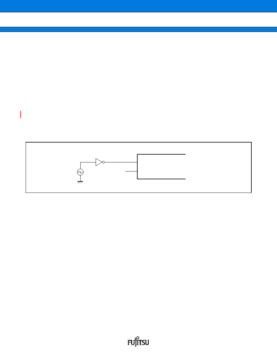
Using External Clock
When using an external clock, drive only X0 pin and leave X1 pin open. An example of using an external clock
is shown below.
Notes When Using No Sub Clock on MB90F897/Y
If an oscillator is not connected to X0A and X1A pins, apply pull-down resistor to the X0A pin and leave the
X1A pin open.
About Power Supply Pins
If two or more Vcc and Vss exist, the pins that should be at the same potential are connected to each other
inside the device. For reducing unwanted emissions and preventing malfunction of strobe signals caused by
increase of ground level, however, be sure to connect the Vcc and Vss pins to the power supply and the ground
externally.
Pay attention to connect a power supply to Vcc and Vss pins of MB90895 series device in a lowest-possible
impedance.
Near pins of MB90895 series device, connecting a bypass capacitor is recommended at 0.1
μF across Vcc
and Vss pins.
Crystal Oscillator Circuit
Noises around X0 and X1 pins cause malfunctions on a MB90895 series device. Design a print circuit so that
X0 and X1 pins, an crystal oscillator (or a ceramic oscillator), and bypass capacitor to the ground become as
close as possible to each other. Furthermore, avoid wires to X0 and X1 pins crossing each other as much as
possible.
Print circuit designing that surrounds X0 and X1 pins with grounding wires, which ensures stable operation,
is strongly recommended.
X1
X0
Open
MB90895 series
Using external clock
相關PDF資料 |
PDF描述 |
|---|---|
| MB90F922NCSPMC | MICROCONTROLLER, PQFP120 |
| MB90F922NCPMC | MICROCONTROLLER, PQFP120 |
| MB90F924NCPMC | MICROCONTROLLER, PQFP120 |
| MB90F946APF | MICROCONTROLLER, PQFP100 |
| MB90F947APF | MICROCONTROLLER, PQFP100 |
相關代理商/技術參數(shù) |
參數(shù)描述 |
|---|---|
| MB90F947APFR-GS-SPE1 | 制造商:FUJITSU 功能描述: |
| MB90F962SPMCR-GE1 | 制造商:FUJITSU 功能描述:IC MCU 16BIT 16LX 48LQFP |
| MB90F962SPMCR-G-JNE1 | 制造商:FUJITSU 功能描述: |
| MB90V340A-102CR | 制造商:FUJITSU 功能描述: |
| MB-910 | 制造商:Circuit Test 功能描述:BREADBOARD WIRING KIT - 350 PCS |
發(fā)布緊急采購,3分鐘左右您將得到回復。