- 您現(xiàn)在的位置:買賣IC網(wǎng) > PDF目錄69021 > MB90F924NCPMC MICROCONTROLLER, PQFP120 PDF資料下載
參數(shù)資料
| 型號: | MB90F924NCPMC |
| 元件分類: | 微控制器/微處理器 |
| 英文描述: | MICROCONTROLLER, PQFP120 |
| 封裝: | 16 X 16 MM, 1.70 MM HEIGHT, 0.50 M PITCH, PLASTIC, LQFP-120 |
| 文件頁數(shù): | 36/72頁 |
| 文件大?。?/td> | 2151K |
| 代理商: | MB90F924NCPMC |
第1頁第2頁第3頁第4頁第5頁第6頁第7頁第8頁第9頁第10頁第11頁第12頁第13頁第14頁第15頁第16頁第17頁第18頁第19頁第20頁第21頁第22頁第23頁第24頁第25頁第26頁第27頁第28頁第29頁第30頁第31頁第32頁第33頁第34頁第35頁當(dāng)前第36頁第37頁第38頁第39頁第40頁第41頁第42頁第43頁第44頁第45頁第46頁第47頁第48頁第49頁第50頁第51頁第52頁第53頁第54頁第55頁第56頁第57頁第58頁第59頁第60頁第61頁第62頁第63頁第64頁第65頁第66頁第67頁第68頁第69頁第70頁第71頁第72頁

MB90920 Series
DS07-13750-3E
41
(Continued)
*5 : Average output current is defined as the average value of the current flowing through any one of the
corresponding pins within a period of 100 ms. The “average value” can be calculated by multiplying the
“operating current” by the “operating factor”.
*6 : Average total output current is defined as the average value of the current flowing through all of the
corresponding pins within a period of 100 ms. The “average value” can be calculated by multiplying the
“operating current” by the “ operating factor”.
*7 :
Applicable to pins: P10 to P15,P50 to P57,P60 to P67,P70 to P77,P80 to P87,PC0 to PC7,PD0 to PD6,
PE0 to PE2
Use within recommended operating conditions.
Use at DC voltage (current) .
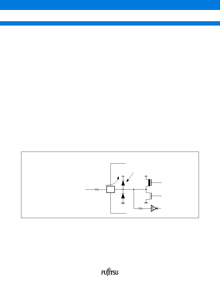
The +B signal should always be applied with a limiting resistance placed between the +B signal and the
microcontroller.
The value of the limiting resistance should be set so that when the +B signal is applied, the input current to
the microcontroller pin does not exceed rated values, either instantaneously or for prolonged periods.
Note that when the microcontroller drive current is low, such as in the power saving modes, the +B input
potential may pass through the protective diode and increase the potential at the VCC pin, and this may affect
other devices.
Note that if a +B signal is input when the microcontroller power supply is off (not fixed at 0 V) , the
microcontroller may partially malfunction on power supplied through the +B signal pin.
Note that if the +B input is applied during power-on, the power supply voltage may reach a level such that
the power-on reset does not function due to the power supplied from the +B signal.
Care must be taken not to leave +B input pins open.
Note that analog system input/output pins (LCD drive pins, comparator input pins, etc.) cannot accept
+B signal inputs.
Sample recommended circuit :
WARNING: Semiconductor devices can be permanently damaged by application of stress (voltage, current,
temperature, etc.) in excess of absolute maximum ratings. Do not exceed these ratings.
P-ch
N-ch
VCC
R
+B input (0 V to 16 V)
Limiting
resistance
Protective diode
Input/output equivalent circuit
相關(guān)PDF資料 |
PDF描述 |
|---|---|
| MB90F946APF | MICROCONTROLLER, PQFP100 |
| MB90F947APF | MICROCONTROLLER, PQFP100 |
| MB90F949APF | MICROCONTROLLER, PQFP100 |
| MB90947APF | MICROCONTROLLER, PQFP100 |
| MB90F947PF | 16-BIT, FLASH, 24 MHz, MICROCONTROLLER, PQFP100 |
相關(guān)代理商/技術(shù)參數(shù) |
參數(shù)描述 |
|---|---|
| MB90F947APFR-GS-SPE1 | 制造商:FUJITSU 功能描述: |
| MB90F962SPMCR-GE1 | 制造商:FUJITSU 功能描述:IC MCU 16BIT 16LX 48LQFP |
| MB90F962SPMCR-G-JNE1 | 制造商:FUJITSU 功能描述: |
| MB90V340A-102CR | 制造商:FUJITSU 功能描述: |
| MB-910 | 制造商:Circuit Test 功能描述:BREADBOARD WIRING KIT - 350 PCS |
發(fā)布緊急采購,3分鐘左右您將得到回復(fù)。