- 您現(xiàn)在的位置:買賣IC網 > PDF目錄377941 > MBM29DL640E90 (Fujitsu Limited) 64 M (8 M X 8/4 M X 16) BIT Dual Operation PDF資料下載
參數(shù)資料
| 型號: | MBM29DL640E90 |
| 廠商: | Fujitsu Limited |
| 英文描述: | 64 M (8 M X 8/4 M X 16) BIT Dual Operation |
| 中文描述: | 64米(8的MX 8 / 4的MX 16)位雙操作 |
| 文件頁數(shù): | 24/71頁 |
| 文件大?。?/td> | 913K |
| 代理商: | MBM29DL640E90 |
第1頁第2頁第3頁第4頁第5頁第6頁第7頁第8頁第9頁第10頁第11頁第12頁第13頁第14頁第15頁第16頁第17頁第18頁第19頁第20頁第21頁第22頁第23頁當前第24頁第25頁第26頁第27頁第28頁第29頁第30頁第31頁第32頁第33頁第34頁第35頁第36頁第37頁第38頁第39頁第40頁第41頁第42頁第43頁第44頁第45頁第46頁第47頁第48頁第49頁第50頁第51頁第52頁第53頁第54頁第55頁第56頁第57頁第58頁第59頁第60頁第61頁第62頁第63頁第64頁第65頁第66頁第67頁第68頁第69頁第70頁第71頁
MBM29DL640E
80/90/12
24
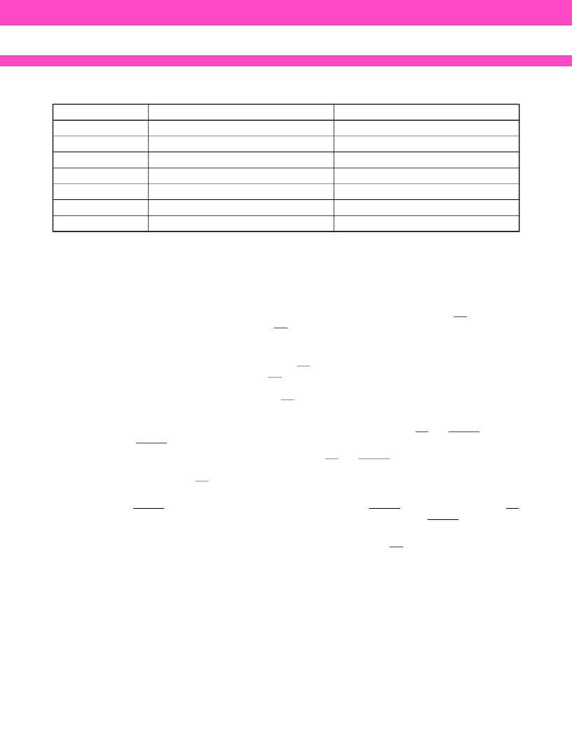
Table 11
Simultaneous Operation
* : By writing erase suspend command on the bank address of sector being erased, the erase operation gets
suspended so that it enables reading from or programming the remaining sectors.
Note: Bank 1 and Bank 2 are divided for the sake of convenience at Simultaneous Operation. Actually, the Bank
consists of 4 banks, Bank A, Bank B, BankC and Bank D. Bank Address (BA) meant to specify each of the
Banks.
Read Mode
The device has two control functions which are required in order to obtain data at the outputs. CE is the power
control and should be used for a device selection. OE is the output control and should be used to gate data to
the output pins.
Address access time (t
ACC
) is equal to delay from stable addresses to valid output data. The chip enable access
time (t
CE
) is the delay from stable addresses and stable CE to valid data at the output pins. The output enable
access time is the delay from the falling edge of OE to valid data at the output pins (assuming the addresses
have been stable for at least t
ACC
-t
OE
time) . When reading out data without changing addresses after power-up,
it is necessary to input hardware reset or to change CE pin from “H” or “L”
Standby Mode
There are two ways to implement the standby mode on the device, one using both the CE and RESET pins, and
the other via the RESET pin only.
When using both pins, a CMOS standby mode is achieved with CE and RESET input held at V
CC
±
0.3 V. Under
this condition the current consumed is less than 5
μ
A Max. During Embedded Algorithm operation, V
CC
active
current (I
CC2
) is required even if CE
=
“H”. The device can be read with standard access time (t
CE
) from either of
these standby modes.
When using the RESET pin only, a CMOS standby mode is achieved with RESET input held at V
SS
±
0.3 V (CE
=
“H” or “L”) . Under this condition the current consumed is less than 5
μ
A Max. Once the RESET pin is set high,
the device requires t
RH
as a wake-up time for output to be valid for read access.
During standby mode, the output is in the high impedance state, regardless of OE input.
Case
Bank 1 Status
Bank 2 Status
1
Read mode
Read mode
2
Read mode
Autoselect mode
3
Read mode
Program mode
4
Read mode
Erase mode *
5
Autoselect mode
Read mode
6
Program mode
Read mode
7
Erase mode *
Read mode
相關PDF資料 |
PDF描述 |
|---|---|
| MBM29DL640E90PBT | 64 M (8 M X 8/4 M X 16) BIT Dual Operation |
| MBM29DL640E90TN | 64 M (8 M X 8/4 M X 16) BIT Dual Operation |
| MBM29DL640E90TR | 64 M (8 M X 8/4 M X 16) BIT Dual Operation |
| MBM29DL64DF | FLASH MEMORY CMOS 64 M (8 M X 8/4 M X 16) BIT |
| MBM29DL64DF-70 | FLASH MEMORY CMOS 64 M (8 M X 8/4 M X 16) BIT |
相關代理商/技術參數(shù) |
參數(shù)描述 |
|---|---|
| MBM29DL640E90PBT | 制造商:FUJITSU 制造商全稱:Fujitsu Component Limited. 功能描述:64 M (8 M X 8/4 M X 16) BIT Dual Operation |
| MBM29DL640E90TN | 制造商:FUJITSU 制造商全稱:Fujitsu Component Limited. 功能描述:64 M (8 M X 8/4 M X 16) BIT Dual Operation |
| MBM29DL640E90TN-LE1 | 制造商:Spansion 功能描述: |
| MBM29DL640E90TR | 制造商:FUJITSU 制造商全稱:Fujitsu Component Limited. 功能描述:64 M (8 M X 8/4 M X 16) BIT Dual Operation |
| MBM29DL64DF | 制造商:FUJITSU 制造商全稱:Fujitsu Component Limited. 功能描述:FLASH MEMORY CMOS 64 M (8 M X 8/4 M X 16) BIT |
發(fā)布緊急采購,3分鐘左右您將得到回復。