- 您現(xiàn)在的位置:買賣IC網(wǎng) > PDF目錄377941 > MBM29DL640E90TR (FUJITSU LTD) 64 M (8 M X 8/4 M X 16) BIT Dual Operation PDF資料下載
參數(shù)資料
| 型號(hào): | MBM29DL640E90TR |
| 廠商: | FUJITSU LTD |
| 元件分類: | DRAM |
| 英文描述: | 64 M (8 M X 8/4 M X 16) BIT Dual Operation |
| 中文描述: | 4M X 16 FLASH 3V PROM, 90 ns, PDSO48 |
| 封裝: | PLASTIC, REVERSE, TSOP1-48 |
| 文件頁(yè)數(shù): | 23/71頁(yè) |
| 文件大小: | 913K |
| 代理商: | MBM29DL640E90TR |
第1頁(yè)第2頁(yè)第3頁(yè)第4頁(yè)第5頁(yè)第6頁(yè)第7頁(yè)第8頁(yè)第9頁(yè)第10頁(yè)第11頁(yè)第12頁(yè)第13頁(yè)第14頁(yè)第15頁(yè)第16頁(yè)第17頁(yè)第18頁(yè)第19頁(yè)第20頁(yè)第21頁(yè)第22頁(yè)當(dāng)前第23頁(yè)第24頁(yè)第25頁(yè)第26頁(yè)第27頁(yè)第28頁(yè)第29頁(yè)第30頁(yè)第31頁(yè)第32頁(yè)第33頁(yè)第34頁(yè)第35頁(yè)第36頁(yè)第37頁(yè)第38頁(yè)第39頁(yè)第40頁(yè)第41頁(yè)第42頁(yè)第43頁(yè)第44頁(yè)第45頁(yè)第46頁(yè)第47頁(yè)第48頁(yè)第49頁(yè)第50頁(yè)第51頁(yè)第52頁(yè)第53頁(yè)第54頁(yè)第55頁(yè)第56頁(yè)第57頁(yè)第58頁(yè)第59頁(yè)第60頁(yè)第61頁(yè)第62頁(yè)第63頁(yè)第64頁(yè)第65頁(yè)第66頁(yè)第67頁(yè)第68頁(yè)第69頁(yè)第70頁(yè)第71頁(yè)
MBM29DL640E
80/90/12
23
I
FUNCTIONAL DESCRIPTION
Simultaneous Operation
The device features functions that enable reading of data from one memory bank while a program or erase
operation is in progress in the other memory bank (simultaneous operation) , in addition to conventional features
(read, program, erase, erase-suspend read, and erase-suspend program) . The bank can be selected by bank
address (A
21
, A
20
, A
19
) with zero latency. The device consists of the following four banks :
Bank A : 8
×
8 KB and 15
×
64 KB; Bank B : 48
×
64 KB; Bank C : 48
×
64 KB; Bank D : 8
×
8 KB and 15
×
64 KB.
The device can execute simultaneous operations between Bank 1, a bank chosen from among the four banks,
and Bank 2, a bank consisting of the three remaining banks. (See Table 9.) This is what we call a “FlexBank”,
for example, the rest of banks B, C and D to let the system read while Bank A is in the process of program (or
erase) operation. However, the different types of operations for the three banks are impossible, e.g. Bank A
writing, Bank B erasing, and Bank C reading out. With this “FlexBank”, as described in Table 10, the system
gets to select from four combinations of data volume for Bank 1 and Bank 2, which works well to meet the system
requirement. The simultaneous operation cannot execute multi-function mode in the same bank. Table 11 shows
the possible combinations for simultaneous operation. (Refer to Figure 11 Bank-to-Bank Read/Write Timing
Diagram.)
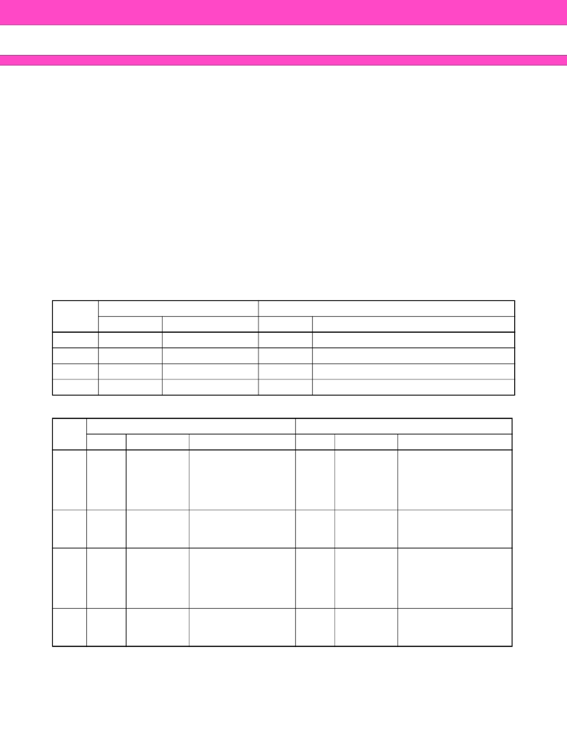
Table 9
FlexBank
TM
Architecture
Table 10
Example of Virtual Banks Combination
Note : When multiple sector erase over several banks is operated, the system cannot read out of the bank to which
a sector being erased belongs. For example, suppose that erasing is taking place at both Bank A and Bank B,
neither Bank A nor Bank B is read out (they would output the sequence flag once they were selected.)
Meanwhile the system would get to read from either Bank C or Bank D.
Bank
Splits
Bank 1
Bank 2
Volume
Combination
Volume
Combination
1
8 Mbit
Bank A
56 Mbit
Remainder (Bank B, C, D)
2
24 Mbit
Bank B
40 Mbit
Remainder (Bank A, C, D)
3
24 Mbit
Bank C
40 Mbit
Remainder (Bank A, B, D)
4
8 Mbit
Bank D
56 Mbit
Remainder (Bank A, B, C)
Bank
Splits
Bank 1
Bank 2
Volume Combination
Sector Size
Volume Combination
Sector Size
1
8 Mbit
Bank A
8
×
8 Kbyte/4 Kword
+
15
×
64 Kbyte/32 Kword
56 Mbit
Bank B
+
Bank C
+
Bank D
8
×
8 Kbyte/4 Kword
+
111
×
64 Kbyte/32 Kword
2
16 Mbit
Bank A
+
Bank D
16
×
8 Kbyte/4 Kword
+
30
×
64 Kbyte/32 Kword
48 Mbit
Bank B
+
Bank C
96
×
64 Kbyte/32 Kword
3
24 Mbit
Bank B
48
×
64 Kbyte/32 Kword 40 Mbit
Bank A
+
Bank C
+
Bank D
16
×
8 Kbyte/4 Kword
+
78
×
64 Kbyte/32 Kword
4
32 Mbit
Bank A
+
Bank B
8
×
8 Kbyte/4 Kword
+
63
×
64 Kbyte/32 Kword
32 Mbit
Bank C
+
Bank D
8
×
8 Kbyte/4 Kword
+
63
×
64 Kbyte/32 Kword
相關(guān)PDF資料 |
PDF描述 |
|---|---|
| MBM29DL64DF | FLASH MEMORY CMOS 64 M (8 M X 8/4 M X 16) BIT |
| MBM29DL64DF-70 | FLASH MEMORY CMOS 64 M (8 M X 8/4 M X 16) BIT |
| MBM29DL64DF70PBT | FLASH MEMORY CMOS 64 M (8 M X 8/4 M X 16) BIT |
| MBM29DL64DF70TN | FLASH MEMORY CMOS 64 M (8 M X 8/4 M X 16) BIT |
| MBM29DL800TA | 8M (1M X 8/512K X 16) BIT |
相關(guān)代理商/技術(shù)參數(shù) |
參數(shù)描述 |
|---|---|
| MBM29DL64DF | 制造商:FUJITSU 制造商全稱:Fujitsu Component Limited. 功能描述:FLASH MEMORY CMOS 64 M (8 M X 8/4 M X 16) BIT |
| MBM29DL64DF-70 | 制造商:FUJITSU 制造商全稱:Fujitsu Component Limited. 功能描述:FLASH MEMORY CMOS 64 M (8 M X 8/4 M X 16) BIT |
| MBM29DL64DF70PBT | 制造商:FUJITSU 制造商全稱:Fujitsu Component Limited. 功能描述:FLASH MEMORY CMOS 64 M (8 M X 8/4 M X 16) BIT |
| MBM29DL64DF70TN | 制造商:FUJITSU 制造商全稱:Fujitsu Component Limited. 功能描述:FLASH MEMORY CMOS 64 M (8 M X 8/4 M X 16) BIT |
| MBM29DL800BA | 制造商:FUJITSU 制造商全稱:Fujitsu Component Limited. 功能描述:8M (1M X 8/512K X 16) BIT |
發(fā)布緊急采購(gòu),3分鐘左右您將得到回復(fù)。