- 您現(xiàn)在的位置:買賣IC網(wǎng) > PDF目錄377948 > MBM29LV008T-X (Fujitsu Limited) CMOS 8M (1M ×8) Flash Memory(CMOS 8M (1M ×8)位3V單電源 閃速存儲器) PDF資料下載
參數(shù)資料
| 型號: | MBM29LV008T-X |
| 廠商: | Fujitsu Limited |
| 英文描述: | CMOS 8M (1M ×8) Flash Memory(CMOS 8M (1M ×8)位3V單電源 閃速存儲器) |
| 中文描述: | 800萬的CMOS(100萬× 8)快閃記憶體(800萬的CMOS(100萬× 8)位3V的單電源閃速存儲器) |
| 文件頁數(shù): | 10/47頁 |
| 文件大小: | 434K |
| 代理商: | MBM29LV008T-X |
第1頁第2頁第3頁第4頁第5頁第6頁第7頁第8頁第9頁當前第10頁第11頁第12頁第13頁第14頁第15頁第16頁第17頁第18頁第19頁第20頁第21頁第22頁第23頁第24頁第25頁第26頁第27頁第28頁第29頁第30頁第31頁第32頁第33頁第34頁第35頁第36頁第37頁第38頁第39頁第40頁第41頁第42頁第43頁第44頁第45頁第46頁第47頁
10
MBM29LV008T-X/MBM29LV008B-X
*1: Outputs 01H at protected sector addresses and outputs 00H at unprotected sector addresses
Write
Device erasure and programming are accomplished via the command register. The contents of the register serve
as inputs to the internal state machine. The state machine outputs dictate the function of the device.
The command register itself does not occupy any addressable memory location. The register is a latch used to
store the commands, along with the address and data information needed to execute the command. The
command register is written by bringing WE to V
IL
, while CE is at V
IL
and OE is at V
IH
. Addresses are latched on
the falling edge of WE or CE, whichever happens later; while data is latched on the rising edge of WE or CE,
whichever happens first. Standard microprocessor write timings are used.
Refer to AC Write Characteristics and the Erase/Programming Waveforms for specific timing parameters.
Sector Protection
The MBM29LV008T-X/008B-X feature hardware sector protection. Those features will disable both program and
erase operations in any number of sectors (0 through 18). The sector protection feature is enabled using
programming equipment at the user's site. Those devices are shipped with all sectors unprotected.
To activate this mode, the programming equipment must force V
ID
on address pin A
9
and control pin OE, (suggest
V
ID
= 11.5 V), CE = V
IL
, and A
6
= V
IL
. The sector addresses (A
19
, A
18
, A
17
, A
16
, A
15
, A
14
, and A
13
) should be set to
the sector to be protected. Tables 4 and 5 define the sector address for each of the nineteen (19) individual
sectors. Programming of the protection circuitry begins on the falling edge of the WE pulse and is terminated
with the rising edge of the same. Sector addresses must be held constant during the WE pulse. Refer to figures
14 and 21 for sector protection waveforms and algorithm.
To verify programming of the protection circuitry, the programming equipment must force V
ID
on address pin A
9
with CE and OE at V
IL
and WE at V
IH
. Scanning the sector addresses (A
19
, A
18
, A
17
, A
16
, A
15
, A
14
, and A
13
) while
(A
10
, A
6
, A
1
, A
0
) = (0, 0, 1, 0) will produce a logical “1” code at device output DQ
0
for a protected sector. Otherwise
the device will read 00H for unprotected sector. In this mode, the lower order addresses, except for A
0
, A
1
, A
6
,
and A
10
are DON’T CARE. Address locations with A
1
= V
IL
are reserved for Autoselect manufacturer and device
codes.
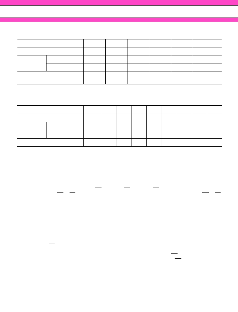
Table 3.1 MBM29LV008T-X/B-X Sector Protection Verify Autoselect Code
Type
A
19
to A
13
A
10
A
6
A
1
A
0
Code (HEX)
Manufacturer’s Code
X
V
IL
V
IL
V
IL
V
IL
04H
Device Code
MBM29LV008T-X
X
V
IL
V
IL
V
IL
V
IH
3EH
MBM29LV008B-X
X
V
IL
V
IL
V
IL
V
IH
37H
Sector Protection
Sector
Addresses
V
IL
V
IL
V
IH
V
IL
01H*
1
Table 3.2 Expanded Autoselect Code Table
Type
Code
DQ
7
DQ
6
DQ
5
DQ
4
DQ
3
DQ
2
DQ
1
DQ
0
Manufacturer’s Code
04H
0
0
0
0
0
1
0
0
Device Code
MBM29LV008T-X
3EH
0
0
1
1
1
1
1
0
MBM29LV008B-X
37H
0
0
1
1
0
1
1
1
Sector Protection
01H
0
0
0
0
0
0
0
1
相關PDF資料 |
PDF描述 |
|---|---|
| MBM29LV008BA | 8M (1M X 8) BIT |
| MBM29LV008BA-90PTR | 8M (1M X 8) BIT |
| MBM29LV008TA-12 | 8M (1M X 8) BIT |
| MBM29LV008TA-12PTN | 8M (1M X 8) BIT |
| MBM29LV008TA-12PTR | 8M (1M X 8) BIT |
相關代理商/技術參數(shù) |
參數(shù)描述 |
|---|---|
| MBM29LV016B | 制造商:FUJITSU 制造商全稱:Fujitsu Component Limited. 功能描述:16M (2M x 8) BIT |
| MBM29LV016B-12 | 制造商:FUJITSU 制造商全稱:Fujitsu Component Limited. 功能描述:16M (2M x 8) BIT |
| MBM29LV016B-12PTN | 制造商:FUJITSU 制造商全稱:Fujitsu Component Limited. 功能描述:16M (2M x 8) BIT |
| MBM29LV016B-12PTR | 制造商:FUJITSU 制造商全稱:Fujitsu Component Limited. 功能描述:16M (2M x 8) BIT |
| MBM29LV016B-80 | 制造商:FUJITSU 制造商全稱:Fujitsu Component Limited. 功能描述:16M (2M x 8) BIT |
發(fā)布緊急采購,3分鐘左右您將得到回復。