- 您現(xiàn)在的位置:買賣IC網(wǎng) > PDF目錄371008 > MC13110AFTA (MOTOROLA INC) UNIVERSAL NARROWBAND FM RECEIVER INTEGRATED CIRCUIT PDF資料下載
參數(shù)資料
| 型號: | MC13110AFTA |
| 廠商: | MOTOROLA INC |
| 元件分類: | 無繩電話/電話 |
| 英文描述: | UNIVERSAL NARROWBAND FM RECEIVER INTEGRATED CIRCUIT |
| 中文描述: | TELECOM, CORDLESS, RF AND BASEBAND CIRCUIT, PQFP48 |
| 封裝: | PLASTIC, LQFP-48 |
| 文件頁數(shù): | 8/68頁 |
| 文件大小: | 1316K |
| 代理商: | MC13110AFTA |
第1頁第2頁第3頁第4頁第5頁第6頁第7頁當(dāng)前第8頁第9頁第10頁第11頁第12頁第13頁第14頁第15頁第16頁第17頁第18頁第19頁第20頁第21頁第22頁第23頁第24頁第25頁第26頁第27頁第28頁第29頁第30頁第31頁第32頁第33頁第34頁第35頁第36頁第37頁第38頁第39頁第40頁第41頁第42頁第43頁第44頁第45頁第46頁第47頁第48頁第49頁第50頁第51頁第52頁第53頁第54頁第55頁第56頁第57頁第58頁第59頁第60頁第61頁第62頁第63頁第64頁第65頁第66頁第67頁第68頁

MC13110A/B MC13111A/B
8
MOTOROLA ANALOG IC DEVICE DATA
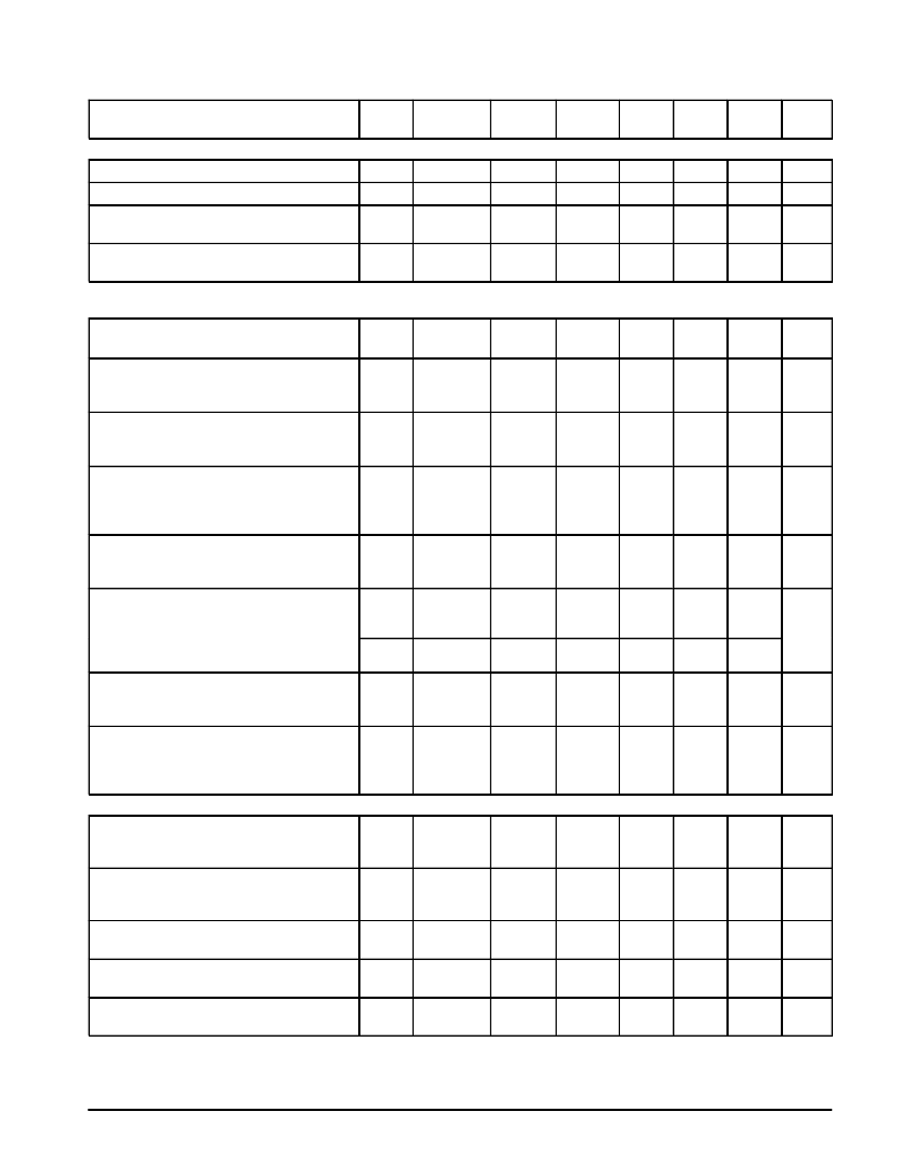
ELECTRICAL CHARACTERISTICS
(continued)
(VCC = 3.6 V, VB = 1.5 V, TA = 25
°
C, Active or Rx Mode, unless otherwise specified;
Test Circuit Figure 1.)
Characteristic
Unit
Max
Typ
Min
Symbol
Measure
Pin
Input
Pin
Figure
Tx AUDIO PATH
(fin = 1.0 kHz, Tx Gain Adj = (01111); ALC, Limiter, and Mutes Disabled; Active Mode, scrambler bypassed)
Low Pass Filter Passband Ripple (Vin = –10 dBV)
1, 84
Maximum Compressor Gain (Vin = –70 dBV)
–
Tx Gain Adjust Range (Programmable through
MPU Interface)
Tx In
C In
Tx Out
Tx Out
Tx Out
Ripple
–
0.7
1.2
dB
AVmax
Tx Range
–
23
–
dB
125
C In
–
–9.0 to
10
–
dB
Tx Gain Adjust Steps – Number of Programmable
Levels
125
C In
Tx Out
Tx n
–
20
–
–
Rx AND Tx SCRAMBLER
(2nd LO = 10.24 MHz, Tx Gain Adj = (01111), Rx Gain Adj = (01111), Volume Control = (0 dB Default Levels),
SCF Clock Divider = 31. Total is divide by 62 for SCF clock frequency of 165.16 kHz)
Rx High Frequency Corner (Note 8)
Rx Path, f = 479 Hz, V Rx Audio In = –20 dBV
–
Rx Audio In
Scr Out
Rx fch
3.55
3.65
3.75
kHz
Tx High Frequency Corner (Note 8)
Tx Path, f = 300 Hz, V Tx In = –10 dBV,
Mic Amp = Unity Gain
–
Tx In
Tx Out
Tx fch
3.829
3.879
3.929
kHz
Absolute Gain
Rx: Vin = –20 dBV
Tx: Vin = –10 dBV, Limiter disabled
–
–
Rx Audio In
Tx In
E Out
Tx Out
AV
–4.0
–4.0
0.4
–1.0
4.0
4.0
dB
Pass Band Ripple
Rx + Tx Path – 1.0
μ
F from Tx Out to
Rx Audio In, fin = low corner frequency to
high corner frequency
–
C In
E Out
Ripple
–
1.9
2.5
dB
Scrambler Modulation Frequency
Rx: 100 mV (–20 dBV)
Tx: 316 mV (–10 dBV)
–
–
Rx Audio In
C In
E Out
Tx Out
fmod
4.119
4.129
4.139
kHz
Group Delay
Rx + Tx Path – 1.0
μ
F from Tx Out to
Rx Audio In, fin = 1.0 kHz
,in
fin = low corner frequency to high corner
frequency
–
C In
E Out
GD
–
1.0
–
ms
–
C In
E Out
GD
–
4.0
–
Carrier Breakthrough
Rx + Tx Path – 1.0
μ
F from Tx Out to
Rx Audio In
–
C In
E Out
CBT
–
–60
–
dB
Baseband Breakthrough
Rx + Tx Path – 1.0
μ
F from Tx Out to
Rx Audio In,
fin = 1.0 kHz, fmeas = 3.192 kHz
–
C In
E Out
BBT
–
–50
–
dB
LOW BATTERY DETECT
Average Threshold
Voltage Before Electronic Adjustment
(Vref_Adj = (0111))
1, 131
Ref1
Ref2
BD1 Out
BD2 Out
VTi
1.38
1.48
1.58
V
Average Threshold
Voltage After Electronic Adjustment
(Vref_Adj = (adjusted value))
1
Ref1
Ref2
BD1 Out
BD2 Out
VTf
1.475
1.5
1.525
V
Hysteresis
–
Ref1
Ref2
BD1 Out
BD2 Out
Hys
–
4.0
–
mV
Input Current (Vin = 1.0 and 2.0 V)
1
–
Ref1
Ref2
Iin
–50
–
50
nA
Output High Voltage (Vin = 2.0 V)
1
Ref1
Ref2
BD1 Out
BD2 Out
VOH
VCC –
0.1
3.6
–
V
NOTE:
8.The filter specification is based on a 10.24 MHz 2nd LO, and a switch–capacitor (SC) filter counter divider ratio of 31. If other 2nd LO frequencies
and/or SC filter counter divider ratios are used, the filter corner frequency will be proportional to the resulting SC filter clock frequency.
相關(guān)PDF資料 |
PDF描述 |
|---|---|
| MC13110BFB | UNIVERSAL NARROWBAND FM RECEIVER INTEGRATED CIRCUIT |
| MC13111AFB | UNIVERSAL NARROWBAND FM RECEIVER INTEGRATED CIRCUIT |
| MC13110BFTA | UNIVERSAL NARROWBAND FM RECEIVER INTEGRATED CIRCUIT |
| MC13111AFTA | UNIVERSAL NARROWBAND FM RECEIVER INTEGRATED CIRCUIT |
| MC13111BFB | UNIVERSAL NARROWBAND FM RECEIVER INTEGRATED CIRCUIT |
相關(guān)代理商/技術(shù)參數(shù) |
參數(shù)描述 |
|---|---|
| MC13110BFB | 制造商:MOTOROLA 制造商全稱:Motorola, Inc 功能描述:UNIVERSAL NARROWBAND FM RECEIVER INTEGRATED CIRCUIT |
| MC13110BFTA | 制造商:Motorola 功能描述:MOTOROLA 9942 |
| MC13111AFB | 制造商:MOTOROLA 制造商全稱:Motorola, Inc 功能描述:UNIVERSAL NARROWBAND FM RECEIVER INTEGRATED CIRCUIT |
| MC13111AFTA | 制造商:MOTOROLA 制造商全稱:Motorola, Inc 功能描述:UNIVERSAL CORDLESS TELEPHONE SUBSYSTEM IC |
| MC13111BFB | 制造商:MOTOROLA 制造商全稱:Motorola, Inc 功能描述:UNIVERSAL NARROWBAND FM RECEIVER INTEGRATED CIRCUIT |
發(fā)布緊急采購,3分鐘左右您將得到回復(fù)。