- 您現(xiàn)在的位置:買(mǎi)賣(mài)IC網(wǎng) > PDF目錄379309 > MC33169 (ON SEMICONDUCTOR) GaAs POWER AMPLIFIER SUPPORT IC PDF資料下載
參數(shù)資料
| 型號(hào): | MC33169 |
| 廠商: | ON SEMICONDUCTOR |
| 英文描述: | GaAs POWER AMPLIFIER SUPPORT IC |
| 中文描述: | 砷化鎵功率放大器支持IC |
| 文件頁(yè)數(shù): | 2/12頁(yè) |
| 文件大小: | 206K |
| 代理商: | MC33169 |
MC33169
2
MOTOROLA ANALOG IC DEVICE DATA
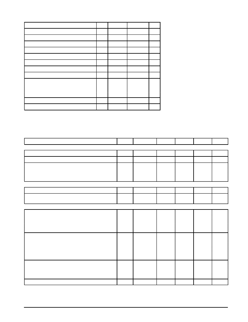
MAXIMUM RATINGS
Rating
Pin
Symbol
Value
Unit
Power Supply Voltage
14
VCC
VTx
Vi
VSense
ISS
Imax
IFmax
IGO
9.5
V
Tx Power Control Input
Idle Mode Input
9
VCC
VCC
–5.0 to 0
V
13
V
Sense Input
10
V
Negative Generator Output Source Current
4
20
mA
Charge Pump Capacitor Current
–
60
mA
Diode Forward Current
–
60
mA
Gate Drive Output Current
8
5.0
mA
Power Dissipation and Thermal Characteristics
Maximum Power Dissipation @ TA = 50
°
C
Thermal Resistance, Junction–to–Air
Operating Junction Temperature
–
PD
R
θ
JA
TJ
TA
Tstg
417
240
+150
mW
°
C/W
°
C
Operating Ambient Temperature
–
–40 to +85
°
C
Storage Temperature Range
–
–60 to +150
°
C
NOTE:
ESD data available upon request.
MC33169–4.0
ELECTRICAL CHARACTERISTICS
(VCC = 4.8 V. For typical values TA = 25
°
C, for min/max values TA is the operating
ambient temperature range that applies, unless otherwise noted.)
Characteristic
Pin
Symbol
Min
Typ
Max
Unit
VBB GENERATOR (VOLTAGE TRIPLER)
Oscillator Frequency
–
fosc
DC
90
100
110
kHz
Oscillator Duty Cycle
–
35
50
65
%
Output Voltage (VCC = 3.0 V, IO = 3.0 mA)
Double Voltage
Triple Voltage
Triple Voltage (VCC = 7.2 V, IO = 3.0 mA)
NEGATIVE GENERATOR OUTPUT
V
12
11
11
VBBD
VBBT
VBBT
4.6
6.1
–
5.0
7.0
11.2
–
–
–
Output Voltage (IO = 3.0 mA)
Output Voltage Ripple with Filter (Rf = 33
, Cf = 4.7
μ
F)
(IO = 0 to 5.0 mA)
PRIORITY MANAGEMENT SECTION
4
VO
Vr
–3.75
–4.0
–4.25
V
4
mVpp
–
2.0
–
Idle Mode Input
Input Voltage High State (Logic 1)
Input Voltage Low State (Logic 0)
Input Current High State (Logic 1)
Input Current Low State (Logic 0), i.e. Standby Mode
13
VIH
VIL
IIH
IIL
2.0
0
10
–
–
–
–
–
2.7
0.5
80
1.0
V
V
μ
A
μ
A
Tx Power Control Input
Input Voltage Range
Input Voltage “Off” State (Zero RF Output Level)
Input Voltage “On” State (Maximum RF Output Level)
Input Resistance
Bandwidth (–3.0 dB)
9
VTx
VTx(off)
VTx(on)
Rin
B
0
–
–
–
–
–
3.1
–
–
–
–
V
V
V
k
MHz
0.7
2.7
90
1.0
Gate Drive Output
Voltage (VTx = 0 V)
Voltage
(VTx = 3.0 V)
Peak Current (Source and Sink) (VTx = 3.0 V)
Undervoltage Lockout Voltage on Sense Input (Magnitude)
8
VGO
–
–
–
0.5
–
–
V
VCC+2.7
–
IGO
Vsense
3.0
mA
10
–3.0
–3.2
–
V
相關(guān)PDF資料 |
PDF描述 |
|---|---|
| MC33169DTB-4.0 | GaAs POWER AMPLIFIER SUPPORT IC |
| MC33215B | Telephone Line Interface and Speakerphone Circuit |
| MC33215FB | Telephone Line Interface and Speakerphone Circuit |
| MC33219ADW | VOICE SWITCHED SPEAKERPHONE CIRCUIT |
| MC33219AP | VOICE SWITCHED SPEAKERPHONE CIRCUIT |
相關(guān)代理商/技術(shù)參數(shù) |
參數(shù)描述 |
|---|---|
| MC33169 | 制造商:SPC Multicomp 功能描述:PTC Resettable Fuse |
| MC33169DTB-004 | 制造商:Rochester Electronics LLC 功能描述:- Bulk |
| MC33169DTB-2.5 | 制造商:MOTOROLA 制造商全稱(chēng):Motorola, Inc 功能描述:GaAs POWER AMPLIFIER SUPPORT IC |
| MC33169DTB-4.0 | 制造商:MOTOROLA 制造商全稱(chēng):Motorola, Inc 功能描述:GaAs POWER AMPLIFIER SUPPORT IC |
| MC3317 | 制造商:MOTOROLA 制造商全稱(chēng):Motorola, Inc 功能描述:Amplifiers and Comparators |
發(fā)布緊急采購(gòu),3分鐘左右您將得到回復(fù)。