- 您現(xiàn)在的位置:買賣IC網(wǎng) > PDF目錄67964 > MC56F8025VLD (FREESCALE SEMICONDUCTOR INC) 16-BIT, FLASH, 32 MHz, MICROCONTROLLER, PQFP44 PDF資料下載
參數(shù)資料
| 型號: | MC56F8025VLD |
| 廠商: | FREESCALE SEMICONDUCTOR INC |
| 元件分類: | 微控制器/微處理器 |
| 英文描述: | 16-BIT, FLASH, 32 MHz, MICROCONTROLLER, PQFP44 |
| 封裝: | 10 X 10 MM, 1.40 MM HEIGHT, 0.80 MM PITCH, ROHS COMPLIANT, MS-026BCB, LQFP-44 |
| 文件頁數(shù): | 147/161頁 |
| 文件大小: | 2160K |
| 代理商: | MC56F8025VLD |
第1頁第2頁第3頁第4頁第5頁第6頁第7頁第8頁第9頁第10頁第11頁第12頁第13頁第14頁第15頁第16頁第17頁第18頁第19頁第20頁第21頁第22頁第23頁第24頁第25頁第26頁第27頁第28頁第29頁第30頁第31頁第32頁第33頁第34頁第35頁第36頁第37頁第38頁第39頁第40頁第41頁第42頁第43頁第44頁第45頁第46頁第47頁第48頁第49頁第50頁第51頁第52頁第53頁第54頁第55頁第56頁第57頁第58頁第59頁第60頁第61頁第62頁第63頁第64頁第65頁第66頁第67頁第68頁第69頁第70頁第71頁第72頁第73頁第74頁第75頁第76頁第77頁第78頁第79頁第80頁第81頁第82頁第83頁第84頁第85頁第86頁第87頁第88頁第89頁第90頁第91頁第92頁第93頁第94頁第95頁第96頁第97頁第98頁第99頁第100頁第101頁第102頁第103頁第104頁第105頁第106頁第107頁第108頁第109頁第110頁第111頁第112頁第113頁第114頁第115頁第116頁第117頁第118頁第119頁第120頁第121頁第122頁第123頁第124頁第125頁第126頁第127頁第128頁第129頁第130頁第131頁第132頁第133頁第134頁第135頁第136頁第137頁第138頁第139頁第140頁第141頁第142頁第143頁第144頁第145頁第146頁當(dāng)前第147頁第148頁第149頁第150頁第151頁第152頁第153頁第154頁第155頁第156頁第157頁第158頁第159頁第160頁第161頁
56F8035/56F8025 Data Sheet, Rev. 6
86
Freescale Semiconductor
6.3.6
SIM Power Control Register (SIM_PWR)
This register controls the Standby mode of the large on-chip regulator. The large on-chip regulator derives
the core digital logic power supply from the IO power supply. At a system bus frequency of 200kHz, the
large regulator may be put in a reduced-power standby mode without interfering with device operation to
reduce device power consumption. Refer to the overview of power-down modes and the overview of clock
generation for more information on the use of large regulator standby.
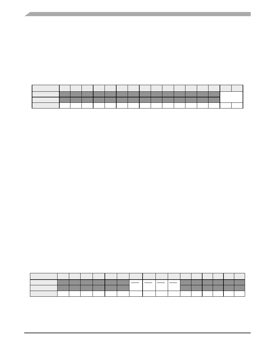
Figure 6-7 SIM Power Control Register (SIM_PWR)
6.3.6.1
Reserved—Bits 15–2
This bit field is reserved. Each bit must be set to 0.
6.3.6.2
Large Regulator Standby Mode (LRSTDBY)—Bits 1–0
00 = Large regulator is in Normal mode
01 = Large regulator is in Standby (reduced-power) mode
10 = Large regulator is in Normal mode and the LRSTDBY field is write-protected until the next reset
11 = Large regulator is in Standby mode and the LRSTDBY field is write-protected until the next reset
6.3.7
Clock Output Select Register (SIM_CLKOUT)
The Clock Output Select register can be used to multiplex out selected clock sources generated inside the
clock generation and SIM modules onto the muxed clock output pins. All functionality is for test purposes
only. Glitches may be produced when the clock is enabled or switched. The delay from the clock source
to the output is unspecified. The observability of the clock output signals at output pads is subject to the
frequency limitations of the associated IO cell.
GPIOA[3:0] can function as GPIO, PWM, or as clock output pins. If GPIOA[3:0] are programmed to
operate as peripheral outputs, then the choice is between PWM and clock outputs. The default state is for
the peripheral function of GPIOA[3:0] to be programmed as PWM (selected by bits [9:6] of the Clock
Output Select register).
See Figure 6-8 for details.
Figure 6-8 CLKO Select Register (SIM_CLKOUT)
Base + $8
15
14
13
12
11
10
9
8
7
6
5
4
3
2
1
0
Read
0
LRSTDBY
Write
RESET
0
000
0
Base + $A
15
14
13
12
11
10
9
8
7
6
5
4
3
2
1
0
Read
0
PWM3PWM2PWM1PWM0
1
0
Write
RESET
0
1
0
0000
相關(guān)PDF資料 |
PDF描述 |
|---|---|
| MC56F8025MLD | 16-BIT, FLASH, 32 MHz, MICROCONTROLLER, PQFP44 |
| MC56F8155VFGE | 4-BIT, 120 MHz, OTHER DSP, PQFP128 |
| MC56F8355VFGE | 4-BIT, 120 MHz, OTHER DSP, PQFP128 |
| MC56F8355MFGE | 4-BIT, 120 MHz, OTHER DSP, PQFP128 |
| MC56F8157VPY | 16-BIT, 120 MHz, OTHER DSP, PQFP160 |
相關(guān)代理商/技術(shù)參數(shù) |
參數(shù)描述 |
|---|---|
| MC56F8025VLDR | 制造商:Freescale Semiconductor 功能描述:16-BIT DSC, 56800E CORE, 32KB FLASH, 32MHZ, QFP 44 - Tape and Reel 制造商:Freescale Semiconductor 功能描述:IC DSC 16BIT 32KB FLASH 44LQFP 制造商:Freescale Semiconductor 功能描述:16 BIT DSPHC |
| MC56F8027 | 制造商:FREESCALE 制造商全稱:Freescale Semiconductor, Inc 功能描述:16-bit Digital Signal Controllers |
| MC56F8027MLH | 功能描述:數(shù)字信號處理器和控制器 - DSP, DSC 16 BIT DSPHC 32KB RoHS:否 制造商:Microchip Technology 核心:dsPIC 數(shù)據(jù)總線寬度:16 bit 程序存儲器大小:16 KB 數(shù)據(jù) RAM 大小:2 KB 最大時(shí)鐘頻率:40 MHz 可編程輸入/輸出端數(shù)量:35 定時(shí)器數(shù)量:3 設(shè)備每秒兆指令數(shù):50 MIPs 工作電源電壓:3.3 V 最大工作溫度:+ 85 C 封裝 / 箱體:TQFP-44 安裝風(fēng)格:SMD/SMT |
| MC56F8027VLD | 制造商:Freescale Semiconductor 功能描述: |
| MC56F8027VLH | 功能描述:數(shù)字信號處理器和控制器 - DSP, DSC 16 BIT DSPHC 32KB RoHS:否 制造商:Microchip Technology 核心:dsPIC 數(shù)據(jù)總線寬度:16 bit 程序存儲器大小:16 KB 數(shù)據(jù) RAM 大小:2 KB 最大時(shí)鐘頻率:40 MHz 可編程輸入/輸出端數(shù)量:35 定時(shí)器數(shù)量:3 設(shè)備每秒兆指令數(shù):50 MIPs 工作電源電壓:3.3 V 最大工作溫度:+ 85 C 封裝 / 箱體:TQFP-44 安裝風(fēng)格:SMD/SMT |
發(fā)布緊急采購,3分鐘左右您將得到回復(fù)。