- 您現(xiàn)在的位置:買賣IC網(wǎng) > PDF目錄299472 > MC56F8123 (Motorola, Inc.) 16-bit Hybrid Controllers PDF資料下載
參數(shù)資料
| 型號: | MC56F8123 |
| 廠商: | Motorola, Inc. |
| 英文描述: | 16-bit Hybrid Controllers |
| 中文描述: | 16位混合控制器 |
| 文件頁數(shù): | 140/140頁 |
| 文件大小: | 1981K |
| 代理商: | MC56F8123 |
第1頁第2頁第3頁第4頁第5頁第6頁第7頁第8頁第9頁第10頁第11頁第12頁第13頁第14頁第15頁第16頁第17頁第18頁第19頁第20頁第21頁第22頁第23頁第24頁第25頁第26頁第27頁第28頁第29頁第30頁第31頁第32頁第33頁第34頁第35頁第36頁第37頁第38頁第39頁第40頁第41頁第42頁第43頁第44頁第45頁第46頁第47頁第48頁第49頁第50頁第51頁第52頁第53頁第54頁第55頁第56頁第57頁第58頁第59頁第60頁第61頁第62頁第63頁第64頁第65頁第66頁第67頁第68頁第69頁第70頁第71頁第72頁第73頁第74頁第75頁第76頁第77頁第78頁第79頁第80頁第81頁第82頁第83頁第84頁第85頁第86頁第87頁第88頁第89頁第90頁第91頁第92頁第93頁第94頁第95頁第96頁第97頁第98頁第99頁第100頁第101頁第102頁第103頁第104頁第105頁第106頁第107頁第108頁第109頁第110頁第111頁第112頁第113頁第114頁第115頁第116頁第117頁第118頁第119頁第120頁第121頁第122頁第123頁第124頁第125頁第126頁第127頁第128頁第129頁第130頁第131頁第132頁第133頁第134頁第135頁第136頁第137頁第138頁第139頁當(dāng)前第140頁
Flash Access Blocking Mechanisms
56F8323 Technical Data, Rev. 11.0
Freescale Semiconductor
99
Preliminary
Proper implementation of Flash security requires that no access to the EOnCE port is provided when
security is enabled. The 56800E core has an input which disables reading of internal memory via the
JTAG/EOnCE. The FM sets this input at reset to a value determined by the contents of the FM security
bytes.
7.2.3
Flash Lockout Recovery
If a user inadvertently enables Flash security on the device, a built-in lockout recovery mechanism can be
used to reenable access to the device. This mechanism completely reases all on-chip Flash, thus disabling
Flash security. Access to this recovery mechanism is built into CodeWarrior via an instruction in memory
configuration (.cfg) files. Add, or uncomment the following configuration command:
unlock_flash_on_connect 1
For more information, please see CodeWarrior MC56F83xx/DSP5685x Family Targeting Manual.
The LOCKOUT_RECOVERY instruction has an associated 7-bit Data Register (DR) that is used to
control the clock divider circuit within the FM module. This divider, FM_CLKDIV[6:0], is used to control
the period of the clock used for timed events in the FM erase algorithm. This register must be set with
appropriate values before the lockout sequence can begin. Refer to the 56F8300 Peripheral User Manual
for more details on setting this register value.
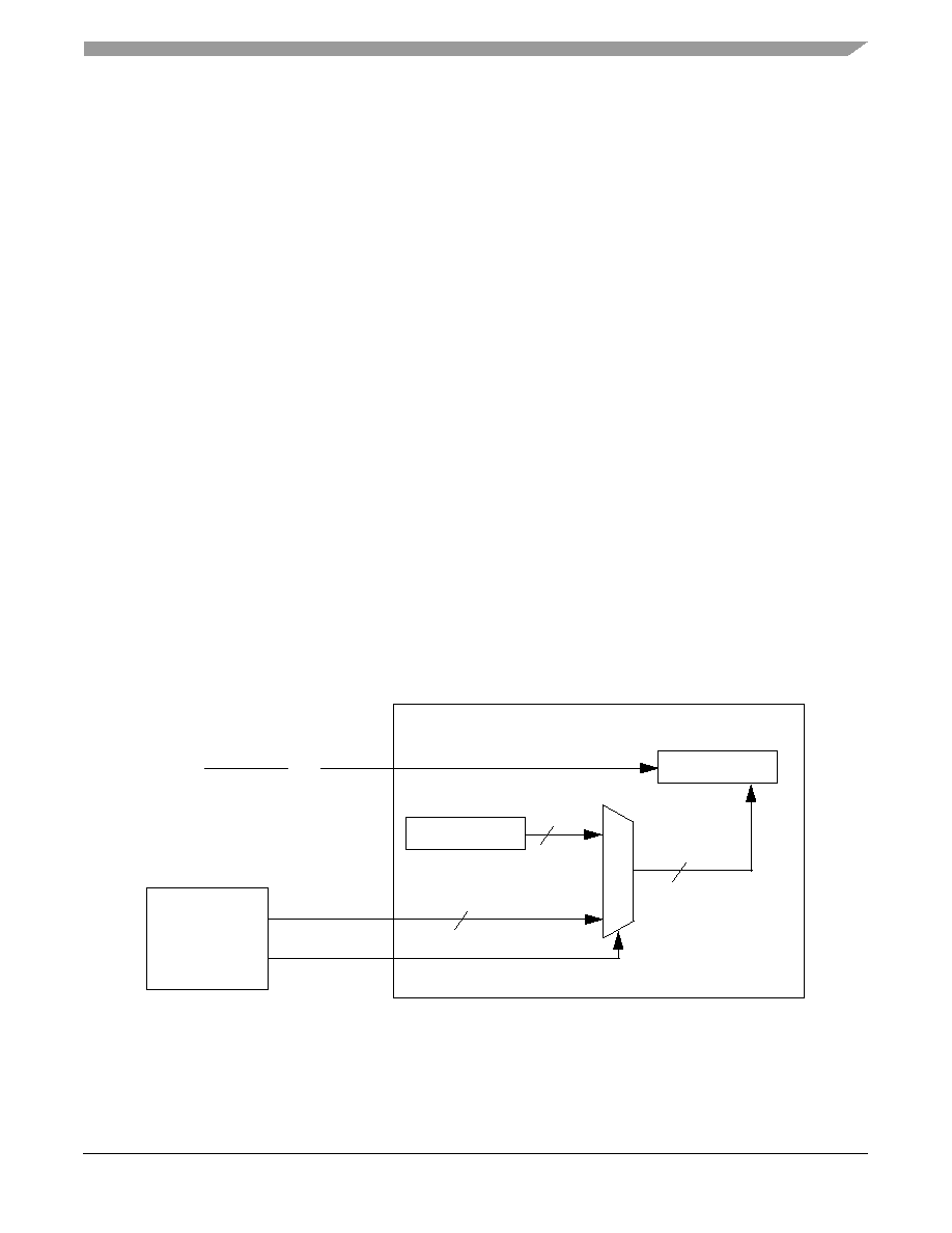
The value of the JTAG FM_CLKDIV[6:0] will replace the value of the FM register FMCLKD that divides
down the system clock for timed events, as illustrated in Figure 7-1. FM_CLKDIV[6] will map to the
PRDIV8 bit, and FM_CLKDIV[5:0] will map to the DIV[5:0] bits. The combination of PRDIV8 and DIV
must divide the FM input clock down to a frequency of 150kHz-200kHz. The “Writing the FMCLKD
Register” section in the Flash Memory chapter of the 56F8300 Peripheral User Manual gives specific
equations for calculating the correct values.
Figure 7-1 JTAG to FM Connection for Lockout Recovery
Two examples of FM_CLKDIV calculations follow.
SYS_CLK
JTAG
FMCLKD
DIVIDER
7
2
FMCLKDIV
FMERASE
Flash Memory
clock
input
相關(guān)PDF資料 |
PDF描述 |
|---|---|
| MC56F8323 | 16-bit Hybrid Controllers |
| MC56MS-14 | 3500 MHz - 12000 MHz RF/MICROWAVE DOUBLE BALANCED MIXER, 9.5 dB CONVERSION LOSS-MAX |
| MC56MS-5 | 3500 MHz - 12000 MHz RF/MICROWAVE DOUBLE BALANCED MIXER, 9.5 dB CONVERSION LOSS-MAX |
| MC68HC11FC0CFU4 | Technical Summary 8-Bit Microcontroller |
| MC68HC11FC0CFU5 | Technical Summary 8-Bit Microcontroller |
相關(guān)代理商/技術(shù)參數(shù) |
參數(shù)描述 |
|---|---|
| MC56F8123VFB | 制造商:MOTOROLA 制造商全稱:Motorola, Inc 功能描述:16-bit Hybrid Controllers |
| MC56F8123VFBE | 功能描述:數(shù)字信號處理器和控制器 - DSP, DSC 16 BIT HYBRID CONTROLLER RoHS:否 制造商:Microchip Technology 核心:dsPIC 數(shù)據(jù)總線寬度:16 bit 程序存儲器大小:16 KB 數(shù)據(jù) RAM 大小:2 KB 最大時鐘頻率:40 MHz 可編程輸入/輸出端數(shù)量:35 定時器數(shù)量:3 設(shè)備每秒兆指令數(shù):50 MIPs 工作電源電壓:3.3 V 最大工作溫度:+ 85 C 封裝 / 箱體:TQFP-44 安裝風(fēng)格:SMD/SMT |
| MC56F8135 | 制造商:FREESCALE 制造商全稱:Freescale Semiconductor, Inc 功能描述:16-bit Digital Signal Controller |
| MC56F8135E | 制造商:FREESCALE 制造商全稱:Freescale Semiconductor, Inc 功能描述:16-bit Digital Signal Controller |
| MC56F8135VFGE | 功能描述:數(shù)字信號處理器和控制器 - DSP, DSC 16 BIT HYBRID CNTRLR RoHS:否 制造商:Microchip Technology 核心:dsPIC 數(shù)據(jù)總線寬度:16 bit 程序存儲器大小:16 KB 數(shù)據(jù) RAM 大小:2 KB 最大時鐘頻率:40 MHz 可編程輸入/輸出端數(shù)量:35 定時器數(shù)量:3 設(shè)備每秒兆指令數(shù):50 MIPs 工作電源電壓:3.3 V 最大工作溫度:+ 85 C 封裝 / 箱體:TQFP-44 安裝風(fēng)格:SMD/SMT |
發(fā)布緊急采購,3分鐘左右您將得到回復(fù)。