- 您現(xiàn)在的位置:買賣IC網(wǎng) > PDF目錄26808 > MC74LCX2952SD (ON SEMICONDUCTOR) LVC/LCX/Z SERIES, 8-BIT REGISTERED TRANSCEIVER, TRUE OUTPUT, PDSO24 PDF資料下載
參數(shù)資料
| 型號(hào): | MC74LCX2952SD |
| 廠商: | ON SEMICONDUCTOR |
| 元件分類: | 總線收發(fā)器 |
| 英文描述: | LVC/LCX/Z SERIES, 8-BIT REGISTERED TRANSCEIVER, TRUE OUTPUT, PDSO24 |
| 封裝: | PLASTIC, SSOP-24 |
| 文件頁(yè)數(shù): | 19/43頁(yè) |
| 文件大小: | 383K |
| 代理商: | MC74LCX2952SD |
第1頁(yè)第2頁(yè)第3頁(yè)第4頁(yè)第5頁(yè)第6頁(yè)第7頁(yè)第8頁(yè)第9頁(yè)第10頁(yè)第11頁(yè)第12頁(yè)第13頁(yè)第14頁(yè)第15頁(yè)第16頁(yè)第17頁(yè)第18頁(yè)當(dāng)前第19頁(yè)第20頁(yè)第21頁(yè)第22頁(yè)第23頁(yè)第24頁(yè)第25頁(yè)第26頁(yè)第27頁(yè)第28頁(yè)第29頁(yè)第30頁(yè)第31頁(yè)第32頁(yè)第33頁(yè)第34頁(yè)第35頁(yè)第36頁(yè)第37頁(yè)第38頁(yè)第39頁(yè)第40頁(yè)第41頁(yè)第42頁(yè)第43頁(yè)
Design Considerations
LCX DATA
BR1339 — REV 3
21
MOTOROLA
Line Driving
With the available high–speed logic families, designers can
reach new heights in system performance. Yet, these faster
devices require a closer look at transmission line effects.
Although all circuit conductors have transmission line
properties, these characteristics become significant when the
edge rates of the drivers are equal to or less than three times
the propagation delay of the line. Significant transmission line
properties may be exhibited in an example where devices
have edge rates of 3ns and lines of 8 inches or greater,
assuming propagation delays of 1.7 ns/ft for an unloaded
printed circuit trace.
Of the many properties of transmission lines, two are of
major interest to the system designer: Zoe, the effective
equivalent impedance of the line, and tpde, the effective
propagation delay down the line. It should be noted that the
intrinsic values of line impedance and propagation delay, Zo
and tpd, are geometry–dependent. Once the intrinsic values
are known, the effects of gate loading can be calculated. The
loaded values for Zoe and tpde can be calculated with:
Zoe +
Zo
1
) C
t Cl
t
pde +
t
pd
1
) C
t Cl
where CI = intrinsic line capacitance and Ct = additional
capacitance due to gate loading.
The formulas indicate that the loading of lines decreases
the effective impedance of the line and increases the
propagation delay. Lines that have a propagation delay
greater than one third the rise time of the signal driver should
be evaluated for transmission line effects. When performing
transmission line analysis on a bus, only the longest, most
heavily loaded and the shortest, least loaded lines need to be
analyzed. All lines in a bus should be terminated equally; if one
line requires termination, all lines in the bus should be
terminated. This will ensure similar signals on all of the lines.
There are several termination schemes which may be
used. Included are series, parallel, AC parallel and Thevenin
terminations. AC parallel and series terminations are the most
useful for low power applications since they do not consume
any DC power. Parallel and Thevenin terminations experience
high DC power consumption.
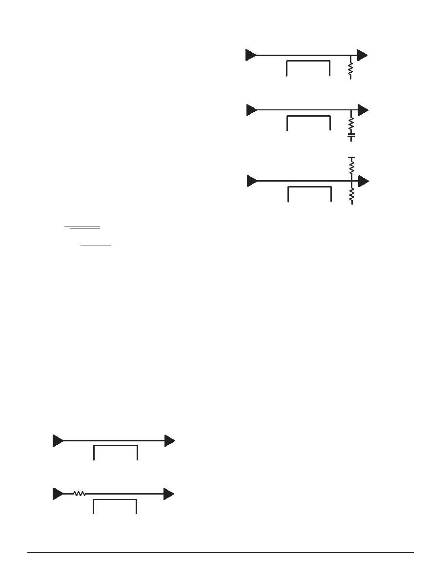
Termination Schemes
a: No Termination
b: Series Termination
Figure 15. Termination Schemes
d: AC Parallel Termination
e: Thevenin Termination
c: Parallel Termination
Series Terminations
Series terminations are most useful in high–speed
applications where most of the loads are at the far end of the
line. Loads that are between the driver and the end of the line
will receive a two–step waveform. The first wave will be the
incident wave. The amplitude is dependent upon the output
impedance of the driver, the value of the series resistor and the
impedance of the line according to the formula
VW = VCC Zoe/(Zoe + RS + ZS)
The amplitude will be one–half the voltage swing if RS (the
series resistor) plus the output impedance (ZS) of the driver is
equal to the line impedance. The second step of the waveform
is the reflection from the end of the line and will have an
amplitude equal to that of the first step. All devices on the line
will receive a valid level only after the wave has propagated
down the line and returned to the driver. Therefore, all inputs
will see the full voltage swing within two times the delay of the
line.
Parallel Termination
Parallel terminations are not generally recommended for
CMOS circuits due to their power consumption, which can
exceed the power consumption of the logic itself. The power
consumption of parallel terminations is a function of the
resistor value and the duty cycle of the signal. In addition,
parallel termination tends to bias the output levels of the driver
towards either VCC or ground. While this feature is not
desirable for driving CMOS inputs, it can be useful for driving
TTL inputs.
AC Parallel Termination
AC parallel terminations work well for applications where
the delays caused by series terminations are unacceptable.
The effects of AC parallel terminations are similar to the effects
of standard parallel terminations. The major difference is that
the capacitor blocks any DC current path and helps to reduce
power consumption.
相關(guān)PDF資料 |
PDF描述 |
|---|---|
| MC74LCX373DTR2 | LVC/LCX/Z SERIES, 8-BIT DRIVER, TRUE OUTPUT, PDSO20 |
| MC74LCX373MR2 | LVC/LCX/Z SERIES, 8-BIT DRIVER, TRUE OUTPUT, PDSO20 |
| MC74LCX540MR2 | LVC/LCX/Z SERIES, 8-BIT DRIVER, INVERTED OUTPUT, PDSO20 |
| MC74LCX540SDR2 | LVC/LCX/Z SERIES, 8-BIT DRIVER, INVERTED OUTPUT, PDSO20 |
| MC74LCX541DTR2 | LVC/LCX/Z SERIES, 8-BIT DRIVER, TRUE OUTPUT, PDSO20 |
相關(guān)代理商/技術(shù)參數(shù) |
參數(shù)描述 |
|---|---|
| MC74LCX32D | 制造商:Rochester Electronics LLC 功能描述:- Bulk |
| MC74LCX32DR2 | 功能描述:邏輯門 2-3.6V Quad 2-Input RoHS:否 制造商:Texas Instruments 產(chǎn)品:OR 邏輯系列:LVC 柵極數(shù)量:2 線路數(shù)量(輸入/輸出):2 / 1 高電平輸出電流:- 16 mA 低電平輸出電流:16 mA 傳播延遲時(shí)間:3.8 ns 電源電壓-最大:5.5 V 電源電壓-最小:1.65 V 最大工作溫度:+ 125 C 安裝風(fēng)格:SMD/SMT 封裝 / 箱體:DCU-8 封裝:Reel |
| MC74LCX32DR2G | 功能描述:邏輯門 2-3.6V Quad 2-Input AND RoHS:否 制造商:Texas Instruments 產(chǎn)品:OR 邏輯系列:LVC 柵極數(shù)量:2 線路數(shù)量(輸入/輸出):2 / 1 高電平輸出電流:- 16 mA 低電平輸出電流:16 mA 傳播延遲時(shí)間:3.8 ns 電源電壓-最大:5.5 V 電源電壓-最小:1.65 V 最大工作溫度:+ 125 C 安裝風(fēng)格:SMD/SMT 封裝 / 箱體:DCU-8 封裝:Reel |
| MC74LCX32DT | 功能描述:邏輯門 2-3.6V Quad 2-Input RoHS:否 制造商:Texas Instruments 產(chǎn)品:OR 邏輯系列:LVC 柵極數(shù)量:2 線路數(shù)量(輸入/輸出):2 / 1 高電平輸出電流:- 16 mA 低電平輸出電流:16 mA 傳播延遲時(shí)間:3.8 ns 電源電壓-最大:5.5 V 電源電壓-最小:1.65 V 最大工作溫度:+ 125 C 安裝風(fēng)格:SMD/SMT 封裝 / 箱體:DCU-8 封裝:Reel |
| MC74LCX32DTEL | 制造商:Rochester Electronics LLC 功能描述:- Bulk |
發(fā)布緊急采購(gòu),3分鐘左右您將得到回復(fù)。