- 您現(xiàn)在的位置:買賣IC網(wǎng) > PDF目錄379319 > MCM67A618B (Motorola, Inc.) 64K x 18 Bit Asynchronous/ Latched Address Fast Static RAM PDF資料下載
參數(shù)資料
| 型號: | MCM67A618B |
| 廠商: | Motorola, Inc. |
| 英文描述: | 64K x 18 Bit Asynchronous/ Latched Address Fast Static RAM |
| 中文描述: | 64K的× 18位異步/鎖存地址快速靜態(tài)存儲器 |
| 文件頁數(shù): | 10/12頁 |
| 文件大小: | 141K |
| 代理商: | MCM67A618B |
MCM67A618B
10
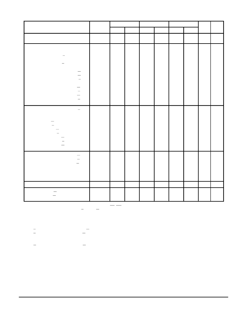
MOTOROLA FAST SRAM
LATCHED WRITE CYCLE TIMING
(See Notes 1, 2, and 3)
MCM67A618B–10
MCM67A618B–12
MCM67A618B–15
Parameter
Symbol
Min
Max
Min
Max
Min
Max
Unit
Notes
Write Cycle Times:
Address Valid to Address Valid
tAVAV
10
—
12
—
15
—
ns
4
Setup Times:
Address Valid to End of Write
Address Valid to End of Write
E Valid to AL Low
Address Valid to AL Low
E Valid to AL High
Address Valid to AL High
AL High to W Low
Address Valid to W Low
Address Valid to E Low
Data Valid to DL Low
Data Valid to W High
Data Valid to E High
DL High to W High
DL High to E High
tAVWH
tAVEH
tEVALL
tAVALL
tEVALH
tAVALH
tALHWL
tAVWL
tAVEL
tDVDLL
tDVWH
tDVEH
tDLHWH
tDLHEH
9
9
2
2
0
0
0
0
0
2
5
5
5
5
—
—
—
—
—
—
—
—
—
—
—
—
—
—
10
10
2
2
0
0
0
0
0
2
6
6
6
6
—
—
—
—
—
—
—
—
—
—
—
—
—
—
13
13
2
2
0
0
0
0
0
2
7
7
7
7
—
—
—
—
—
—
—
—
—
—
—
—
—
—
ns
Hold Times:
AL Low to E High
AL Low to Address Invalid
DL Low to Data Invalid
W High to Address Invalid
E High to Address Invalid
W High to Data Invalid
E High to Data Invalid
W High to DL High
E High to DL High
W High to AL High
tALLEH
tALLAX
tDLLDX
tWHAX
tEHAX
tWHDX
tEHDX
tWHDLH
tEHDLH
tWHALH
2
2
2
0
0
0
0
0
0
0
—
—
—
—
—
—
—
—
—
—
2
2
2
0
0
0
0
0
0
0
—
—
—
—
—
—
—
—
—
—
3
3
3
0
0
0
0
0
0
0
—
—
—
—
—
—
—
—
—
—
ns
4
4
Write Pulse Width:
AL High to W High
Write Pulse Width (G Low)
Write Pulse Width (G High)
Write Pulse Width
Enable to End of Write
Enable to End of Write
tALHWH
tWLWH
tWLWH
tWLEH
tELWH
tELEH
9
9
8
9
9
9
—
—
—
—
—
—
10
10
9
10
10
10
—
—
—
—
—
—
13
13
12
13
13
13
—
—
—
—
—
—
ns
5
6
7
6, 7
Address Latch Pulse Width
tALHALL
5
—
5
—
5
—
ns
4
Output Buffer Control:
W High to Output Active
W Low to Output High–Z
tWHQX
tWLQZ
3
—
—
5
3
—
—
6
3
—
—
9
ns
8
8, 9
NOTES:
1. W (write) refers to either one or both byte write enables (LW, UW).
2. A write occurs during the overlap of E low and W low.
3. Both Write Enables must be equal to VIH for all address transitions.
4. All write cycle timing is referenced from the last valid address to the first transitioning address.
5. All latched inputs must meet the specified setup and hold times with stable logic levels for ALL falling edges of address latch (AL) and data
latch (DL).
6. If E goes high coincident with or before W goes high the output will remain in a high impedance state.
7. If E goes low coincident with or after W goes low the output will remain in a high impedance state.
8. Transition is measured
±
500 mV from steady–state voltage with output load of Figure 1b. This parameter is sampled and not 100% tested.
At any given voltage and temperature, tWLQZ is less than tWHQX for a given device.
9. If G goes low coincident with or after W goes low the output will remain in a high impedance state.
相關(guān)PDF資料 |
PDF描述 |
|---|---|
| MCM67A618BFN10 | 64K x 18 Bit Asynchronous/ Latched Address Fast Static RAM |
| MCM67A618BFN12 | THERMISTORS |
| MCM67A618BFN15 | 64K x 18 Bit Asynchronous/ Latched Address Fast Static RAM |
| MCM67M618B | 64K x 18 Bit BurstRAM Synchronous Fast Static RAM |
| MCM67M618BFN10 | 64K x 18 Bit BurstRAM Synchronous Fast Static RAM |
相關(guān)代理商/技術(shù)參數(shù) |
參數(shù)描述 |
|---|---|
| MCM67A618BFN10 | 制造商:MOTOROLA 制造商全稱:Motorola, Inc 功能描述:64K x 18 Bit Asynchronous/ Latched Address Fast Static RAM |
| MCM67A618BFN12 | 制造商:MOTOROLA 制造商全稱:Motorola, Inc 功能描述:64K x 18 Bit Asynchronous/ Latched Address Fast Static RAM |
| MCM67A618BFN15 | 制造商:MOTOROLA 制造商全稱:Motorola, Inc 功能描述:64K x 18 Bit Asynchronous/ Latched Address Fast Static RAM |
| MCM67A618FN10 | 制造商:MOTOROLA 制造商全稱:Motorola, Inc 功能描述:64K x 18 Bit Asychronous/Latched Address Fast Static RAM |
| MCM67A618FN12 | 制造商:MOTOROLA 制造商全稱:Motorola, Inc 功能描述:64K x 18 Bit Asychronous/Latched Address Fast Static RAM |
發(fā)布緊急采購,3分鐘左右您將得到回復(fù)。