- 您現(xiàn)在的位置:買賣IC網(wǎng) > PDF目錄377963 > MD1711 (Supertex, Inc.) HIGH SPEED INTEGRATED ULTRASOUND DRIVER IC PDF資料下載
參數(shù)資料
| 型號(hào): | MD1711 |
| 廠商: | Supertex, Inc. |
| 英文描述: | HIGH SPEED INTEGRATED ULTRASOUND DRIVER IC |
| 中文描述: | 高速集成電路超聲驅(qū)動(dòng)IC |
| 文件頁數(shù): | 1/9頁 |
| 文件大小: | 192K |
| 代理商: | MD1711 |
MD1711
Initial Release
Rev.12 011005
1
High Speed, Integrated Ultrasound Driver IC
Features
Drives two ultrasound transducer channels
Generates 5-level waveform
Drives 12 high voltage MOSFETs
±2.0A source and sink peak current
Up to 20MHz output frequency
12V/ns slew rate
±3ns matched delay times
Second harmonic is less than -40dB
Two separate gate drive voltages
1.8V to 3.3V CMOS logic interface
Applications
Medical ultrasound imaging
Piezoelectric transducer drivers
Metal flaw detection
Nondestructive evaluation
Sonar Transmitter
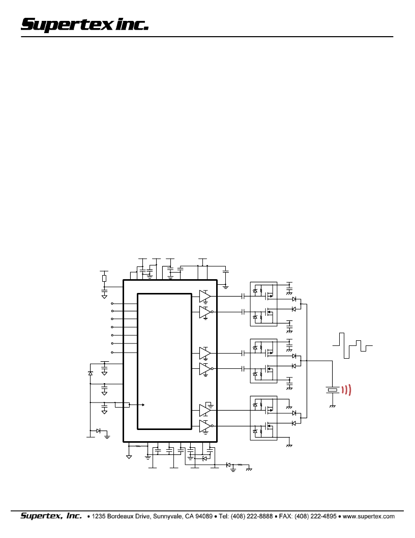
Typical Application Circuit (1 of 2 Channels)
General Description
The Supertex MD1711 is an IC for a two-channel, 5-
level, high voltage and high-speed transmitter driver.
It is designed for medical ultrasound imaging
applications but can also be used for metal flaw
detection, nondestructive evaluation, and driving
piezoelectric transducers.
The MD1711 is a two-channel logic controller circuit
with low impedance MOSFET gate drivers. There are
two sets of control logic inputs, one for channel A and
one for Channel B. Each channel consists of three
pairs of MOSFET gate drivers. These drivers are
designed to match the drive requirements of the
Supertex TC6320. The MD1711 drives six TC6320s.
Each pair an N-channel and a P-channel MOSFET.
They are designed to have the same impedance and
can provide peak currents of over 2.0 amps
.
NR012505
V
NN
1
TC6320
+100V
-100V
+50V
-50V
0V
0V
30
32
34
44
39
41
37
DV DD2
DVDD2
DV DD1
DVDD1
V
SS
DVDD1
D
VSS
-10V
DV
DD
1
DV
DD
2
26
16
19
21
+10V
VL L
+3 .3V
AV S S
48
14
15
AV
SS
SEL
POSA / POS1A
EN
DGND
AGND
7
0
MD1711
(1/2 of I/O)
SU B
18
AV S S
33
36
28
25
31
DGND
35
40
42
43
DV
SS
45
FB
AV
DD
1
6
0
46
47
13
1
2
3
4
5
OUTPA1
OUTNA1
OUTPA2
OUTNA2
OUTPA3
OU
TNA3
DGND
DGND
+5V
DV
DD
1
+1 0V
DV
DD
2
+5 V
+10V
+1 0V
DGND
+10V
-10V
-10V
DV
DD
2
DV
DD
1
DV
DD
1
Transducer
0.22
μ
F
Control Logic
& Level
Translator
NEGA / NEG1A
HVEN1A / POS2A
HVEN2A / NEG2A
ClampA
0.1
μ
F
0.1
μ
F
0.1
μ
F
0.22
μ
F
0.22
μ
F
0.22
μ
F
0.22
μ
F
0.22
μ
F
0.1
μ
F
10nF
10nF
10nF
10nF
1
μ
F
1
μ
F
1
μ
F
1
μ
F
V
NN
2
V
PP
2
V
PP
1
相關(guān)PDF資料 |
PDF描述 |
|---|---|
| MD1711FG | HIGH SPEED INTEGRATED ULTRASOUND DRIVER IC |
| MD1802FH | High voltage NPN Power transistor for standard Definition CRT display |
| MD1802FX | High voltage NPN Power transistor for standard Definition CRT display |
| MD1803DFH | High voltage NPN Power transistor for standard Definition CRT display |
| MD1803DFH_0609 | High voltage NPN Power transistor for standard Definition CRT display |
相關(guān)代理商/技術(shù)參數(shù) |
參數(shù)描述 |
|---|---|
| MD1711_07 | 制造商:SUPERTEX 制造商全稱:SUPERTEX 功能描述:High Speed, Integrated Ultrasound Driver IC |
| MD1711DB1 | 功能描述:電源管理IC開發(fā)工具 MD1711 + TC6320 Demo Board RoHS:否 制造商:Maxim Integrated 產(chǎn)品:Evaluation Kits 類型:Battery Management 工具用于評(píng)估:MAX17710GB 輸入電壓: 輸出電壓:1.8 V |
| MD1711DB2 | 功能描述:電源管理IC開發(fā)工具 MD1711 + TC6320 DEMOBOARD RoHS:否 制造商:Maxim Integrated 產(chǎn)品:Evaluation Kits 類型:Battery Management 工具用于評(píng)估:MAX17710GB 輸入電壓: 輸出電壓:1.8 V |
| MD1711FG | 功能描述:功率驅(qū)動(dòng)器IC Hi-Spd Ultrasound RoHS:否 制造商:Micrel 產(chǎn)品:MOSFET Gate Drivers 類型:Low Cost High or Low Side MOSFET Driver 上升時(shí)間: 下降時(shí)間: 電源電壓-最大:30 V 電源電壓-最小:2.75 V 電源電流: 最大功率耗散: 最大工作溫度:+ 85 C 安裝風(fēng)格:SMD/SMT 封裝 / 箱體:SOIC-8 封裝:Tube |
| MD1711FG-G | 功能描述:功率驅(qū)動(dòng)器IC Hi-Spd Ultrasound RoHS:否 制造商:Micrel 產(chǎn)品:MOSFET Gate Drivers 類型:Low Cost High or Low Side MOSFET Driver 上升時(shí)間: 下降時(shí)間: 電源電壓-最大:30 V 電源電壓-最小:2.75 V 電源電流: 最大功率耗散: 最大工作溫度:+ 85 C 安裝風(fēng)格:SMD/SMT 封裝 / 箱體:SOIC-8 封裝:Tube |
發(fā)布緊急采購,3分鐘左右您將得到回復(fù)。