- 您現(xiàn)在的位置:買賣IC網(wǎng) > PDF目錄359164 > MGCM02BP1N (Zarlink Semiconductor Inc.) TDMA/AMPS IF and Baseband Interface PDF資料下載
參數(shù)資料
| 型號(hào): | MGCM02BP1N |
| 廠商: | Zarlink Semiconductor Inc. |
| 英文描述: | TDMA/AMPS IF and Baseband Interface |
| 中文描述: | 時(shí)分多址/ AMPS二元IF和基帶接口 |
| 文件頁(yè)數(shù): | 10/21頁(yè) |
| 文件大小: | 529K |
| 代理商: | MGCM02BP1N |
第1頁(yè)第2頁(yè)第3頁(yè)第4頁(yè)第5頁(yè)第6頁(yè)第7頁(yè)第8頁(yè)第9頁(yè)當(dāng)前第10頁(yè)第11頁(yè)第12頁(yè)第13頁(yè)第14頁(yè)第15頁(yè)第16頁(yè)第17頁(yè)第18頁(yè)第19頁(yè)第20頁(yè)第21頁(yè)
MGCM02
Data Sheet
10
band pass
fi
lter. This can be provided in two ways as
described in the preceding FM section.
In the
fi
xed gain FM mode the RSSI output is input to
a comparator. The output of this comparator then
reduces the IF ampli
fi
er gain by 32.5dB thus
enabling a larger dynamic range for the RSSI.
Hysteresis is built in to prevent oscillation when close
to the threshold level. Fig 6 shows the RSSI
characteristic. At low signal levels the RSSI output
increases with signal level, however at high signal
level when the gain is reduced in the input path, the
RSSI output is mirrored around Vdd/2 and decreases
with increasing signal level. The slope is the same at
high level as at low level but is of course negative.
The actual slope (or gain) and settling time for the
RSSI are set by external components as shown in
fi
g
5.
The RSSI output from the MGCM02 will normally be
input into an a to d converter. This, together with the
baseboard controller can convert the RSSI signal to
a monotonic digital output as required by the IS136
speci
fi
cations. Calibration will be required to
determine the slope, offset at low and high signal
levels, and threshold level of the RSSI characteristic.
For example if the RSSI output is less than Vdd/2
then the RSSI slope is positive; if greater than Vdd/2
than the RSSI slope is negative.
If the AGC mode is used for FM then this automatic
RSSI switching is disabled and the RSSI is only
operated
over
the
lower
characteristic. The actual signal level must then be
calculated by the baseband using the measured
RSSI level and the applied AGC signal.
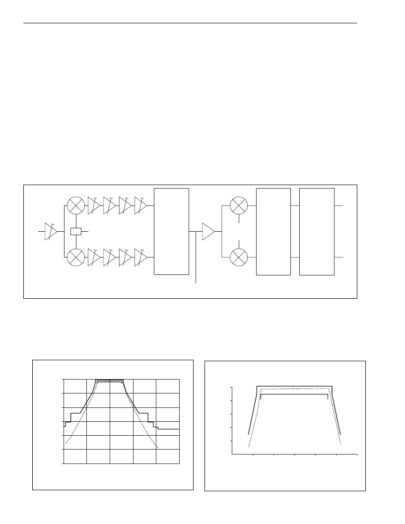
segment
of
the
60 kHz
60 kHz
I
Q
To FM Discriminator
and RSSI
90
∞
Rx LO
60 kHz
60kHz
Band Pass
Switched
Capacitor
Chebychev
n = 5
BW
= +/- 16kHz
G =14dB
Low Pass
Switched
Capacitor
Chebychev
n = 3
BW = 37.5kHz
G = 8dB
Smoothing
Filter
Low Pass
Butterworth
n = 2
BW = 60 kHz
G = 6 dB
14dB
Each gain stage is
programmable from -12dB to
+12 dB in 0.5dB increments
IF
Input
Gain
Settings
-2dB
6dB
12dB
21.6dB
Figure 2 - Receive Path Block Diagram showing Gain Plan and Filters
Filter Response
0
20
40
60
80
100
120
0
30
60
90
120
150
Frequency (kHz)
A
Passband Detail
0
5
10
15
20
25
30
40
50
60
70
80
90
Frequency (kHz)
A
Figure 3 - Band Pass Filter Response
相關(guān)PDF資料 |
PDF描述 |
|---|---|
| MGCM02BP1Q | TDMA/AMPS IF and Baseband Interface |
| MGCM02KG | TDMA/AMPS IF and Baseband Interface |
| MGCT04LH1S | Transmit Circuit for TDMA/AMPS and CDMA/AMPS |
| MGCT04LH1T | Transmit Circuit for TDMA/AMPS and CDMA/AMPS |
| MGCT04 | Transmit Circuit for TDMA/AMPS and CDMA/AMPS |
相關(guān)代理商/技術(shù)參數(shù) |
參數(shù)描述 |
|---|---|
| MGCM02BP1Q | 制造商:ZARLINK 制造商全稱:Zarlink Semiconductor Inc 功能描述:TDMA/AMPS IF and Baseband Interface |
| MGCM02KG | 制造商:ZARLINK 制造商全稱:Zarlink Semiconductor Inc 功能描述:TDMA/AMPS IF and Baseband Interface |
| MGCOV | 功能描述:繼電器插座與硬件 RELAY COVER RoHS:否 制造商:TE Connectivity / Schrack 附件類型:Socket 相關(guān)繼電器系列:RP, RT, RY 端接類型:PCB 極數(shù):1 |
| MGCR01 | 制造商:ZARLINK 制造商全稱:Zarlink Semiconductor Inc 功能描述:Dual Mode IF Receiver for TDMA/AMPS and CDMA/AMPS |
| MGCR01KG | 制造商:ZARLINK 制造商全稱:Zarlink Semiconductor Inc 功能描述:Dual Mode IF Receiver for TDMA/AMPS and CDMA/AMPS |
發(fā)布緊急采購(gòu),3分鐘左右您將得到回復(fù)。