- 您現(xiàn)在的位置:買賣IC網(wǎng) > PDF目錄377970 > ML4805CS (FAIRCHILD SEMICONDUCTOR CORP) Variable Feedforward PFC/PWM Controller Combo PDF資料下載
參數(shù)資料
| 型號: | ML4805CS |
| 廠商: | FAIRCHILD SEMICONDUCTOR CORP |
| 元件分類: | 穩(wěn)壓器 |
| 英文描述: | Variable Feedforward PFC/PWM Controller Combo |
| 中文描述: | 0.5 A POWER FACTOR CONTROLLER WITH POST REGULATOR, 212 kHz SWITCHING FREQ-MAX, PDSO18 |
| 封裝: | PLASTIC, SOIC-18 |
| 文件頁數(shù): | 10/13頁 |
| 文件大?。?/td> | 125K |
| 代理商: | ML4805CS |
ML4805
10
REV. 1.1 3/9/2001
Generating V
CC
The ML4805 is a voltage-fed part. It requires an external
15V
±
10% or better Zener shunt voltage regulator, or some
other controlled supply, to regulate the voltage supplied
to the part at 15V nominal. This allows a low power
dissipation while at the same time delivering 13V
nominal of gate drive at the PWM OUT and PFC OUT
outputs. If using a Zener diode, it is important to limit the
current through the Zener to avoid overheating or
destroying it. This can be easily done with a single resistor
in series with the Vcc pin, returned to a bias supply of
typically 18V to 20V. The resistor
’
s value must be chosen
to meet the operating current requirement of the ML4805
itself (8.5mA max.) plus the current required by the two
gate driver outputs.
EXAMPLE:
With a V
BIAS
of 20V, a V
CC
limit of 16.5V (max) and
driving a total gate charge of 110nC at 100kHz (1 IRF840
MOSFET and 2 IRF830 MOSFETs), the gate driver current
required is:
The ML4805 should be locally bypassed with a 10nF and
a 1
μ
F ceramic capacitor. In most applications, an
electrolytic capacitor of between 100
μ
F and 330
μ
F is also
required across the part, both for filtering and as part of
the start-up bootstrap circuitry.
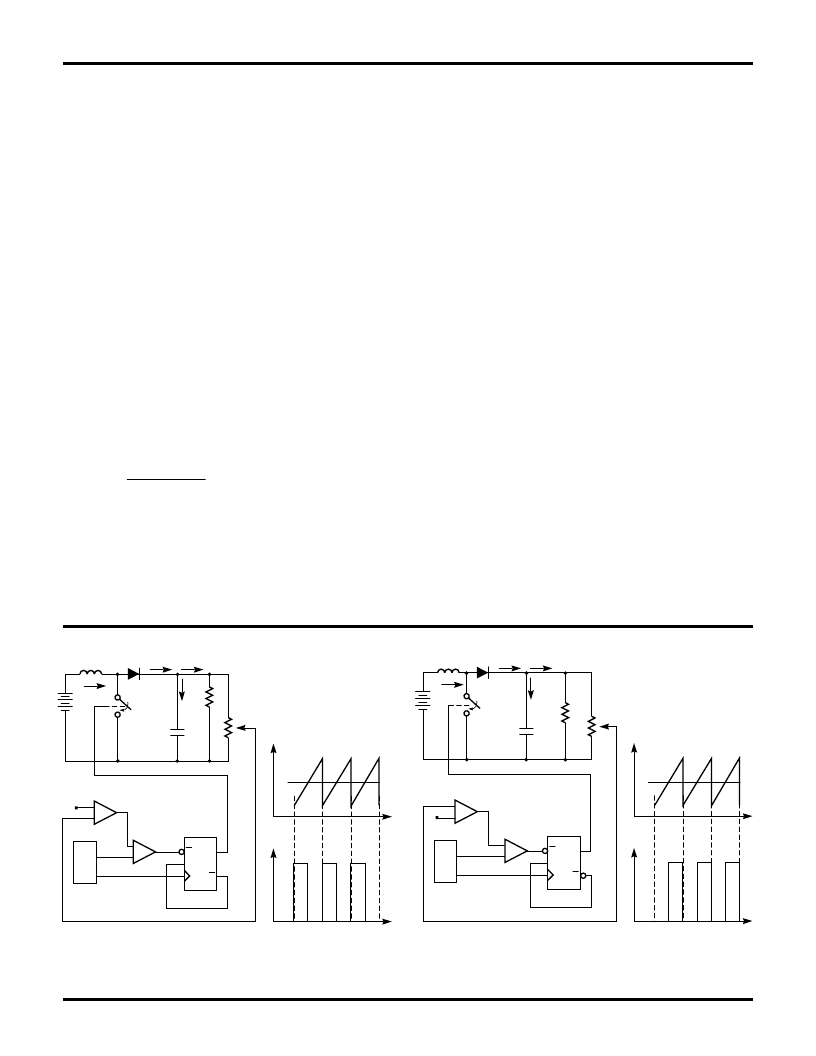
LEADING/TRAILING MODULATION
Conventional Pulse Width Modulation (PWM) techniques
employ trailing edge modulation in which the switch will
turn on right after the trailing edge of the system clock.
The error amplifier output voltage is then compared with
the modulating ramp. When the modulating ramp reaches
the level of the error amplifier output voltage, the switch
will be turned OFF. When the switch is ON, the inductor
current will ramp up. The effective duty cycle of the
trailing edge modulation is determined during the ON
time of the switch. Figure 3 shows a typical trailing edge
control scheme.
In the case of leading edge modulation, the switch is
turned OFF right at the leading edge of the system clock.
When the modulating ramp reaches the level of the error
amplifier output voltage, the switch will be turned ON.
The effective duty-cycle of the leading edge modulation
is determined during the OFF time of the switch. Figure 4
shows a leading edge control scheme.
One of the advantages of this control technique is that it
requires only one system clock. Switch 1 (SW1) turns off
and switch 2 (SW2) turns on at the same instant to
minimize the momentary
“
no-load
”
period, thus lowering
ripple voltage generated by the switching action. With
such synchronized switching, the ripple voltage of the
first stage is reduced. Calculation and evaluation have
shown that the 120Hz component of the PFC
’
s output
ripple voltage can be reduced by as much as 30% using
this method.
FUNCTIONAL DESCRIPTION
(Continued)
Figure 4. Leading/Trailing Edge Control Scheme
Figure 3. Typical Trailing Edge Control Scheme
RAMP
VEAO
TIME
VSW1
TIME
REF
EA
–
+
–
+
OSC
DFF
R
D
Q
Q
CLK
U1
RAMP
CLK
U4
U3
C1
RL
I4
SW2
SW1
+
DC
I1
I2
I3
VIN
L1
U2
REF
EA
–
+
–
+
OSC
DFF
R
D
Q
Q
CLK
U1
RAMP
CLK
U4
U3
C1
RL
I4
SW2
SW1
+
DC
I1
I2
I3
VIN
L1
VEAO
CMP
U2
RAMP
VEAO
TIME
VSW1
TIME
!"#
'
(
相關(guān)PDF資料 |
PDF描述 |
|---|---|
| ML4805IP | Variable Feedforward PFC/PWM Controller Combo |
| ML4805IS | Variable Feedforward PFC/PWM Controller Combo |
| ML4810 | High Frequency PWM Controller(高頻PWM控制器) |
| ML4811 | High Frequency PWM Controller(高頻PWM控制器) |
| ML4812IQ | Power Factor Controller |
相關(guān)代理商/技術(shù)參數(shù) |
參數(shù)描述 |
|---|---|
| ML4805CSX | 功能描述:功率因數(shù)校正 IC SOIC-WIDE-18 RoHS:否 制造商:Fairchild Semiconductor 開關(guān)頻率:300 KHz 最大功率耗散: 最大工作溫度:+ 125 C 安裝風(fēng)格:SMD/SMT 封裝 / 箱體:SOIC-8 封裝:Reel |
| ML4805IP | 制造商:MICRO-LINEAR 制造商全稱:MICRO-LINEAR 功能描述:Variable Feedforward PFC/PWM Controller Combo |
| ML4805IS | 制造商:MICRO-LINEAR 制造商全稱:MICRO-LINEAR 功能描述:Variable Feedforward PFC/PWM Controller Combo |
| ML4810 | 制造商:MICRO-LINEAR 制造商全稱:MICRO-LINEAR 功能描述:High Frequency Power Supply Controller |
| ML4810CP | 制造商:MICRO-LINEAR 制造商全稱:MICRO-LINEAR 功能描述:High Frequency Power Supply Controller |
發(fā)布緊急采購,3分鐘左右您將得到回復(fù)。