- 您現(xiàn)在的位置:買賣IC網(wǎng) > PDF目錄377972 > ML671000 (OKI SEMICONDUCTOR CO., LTD.) CMOS 32-Bit Single-Chip Microcontroller with Built-in USB Device Controller(內(nèi)置USB設(shè)備控制器的32位單芯片微控制器) PDF資料下載
參數(shù)資料
| 型號: | ML671000 |
| 廠商: | OKI SEMICONDUCTOR CO., LTD. |
| 英文描述: | CMOS 32-Bit Single-Chip Microcontroller with Built-in USB Device Controller(內(nèi)置USB設(shè)備控制器的32位單芯片微控制器) |
| 中文描述: | 的CMOS 32位單片機具有內(nèi)置的USB設(shè)備控制器(內(nèi)置的USB設(shè)備控制器的32位單芯片微控制器) |
| 文件頁數(shù): | 7/25頁 |
| 文件大小: | 261K |
| 代理商: | ML671000 |
FEDL671000-02
1
Semiconductor
ML671000
7/25
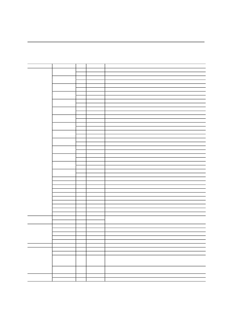
PIN DESCRIPTION (3)
Classification
Pin Name
I/O
I/O
O
I/O
O
I/O
I
I/O
I
I/O
I
I/O
I
I/O
O
I/O
O
I/O
O
I/O
I
I/O
O
I/O
O
I/O
I
I/O
I
I/O
I/O
I/O
I/O
I/O
I/O
I/O
I/O
I/O
I/O
I/O
I/O
I
I
I
O
I
I
I
I
Function
Primary
Secondary
Primary
Secondary
Primary
Secondary
Primary
Secondary
Primary
Secondary
Primary
Secondary
Primary
Secondary
Primary
Secondary
Primary
Secondary
Primary
Secondary
Primary
Secondary
Primary
Secondary
Primary
Secondary
Primary
Secondary
—
—
—
—
—
—
—
—
—
—
—
—
—
—
—
—
—
—
—
—
Description
Bit 7 of port 5
DTR signal output pin for UART serial port
Bit 6 of port 5
RTS signal output pin for UART serial port
Bit 5 of port 5
CTS signal input pin for UART serial port
Bit 4 of port 5
DSR signal input pin for UART serial port
Bit 3 of port 5
DCD signal input pin for UART serial port
Bit 2 of port 5
RI signal input pin for UART serial port
Bit 1 of port 5
OUT1 signal output pin for UART serial port
Bit 0 of port 5
OUT2 signal output pin for UART serial port
Bit 7 of port 6
Bus release request acknowledged signal output pin
Bit 6 of port 6
Bus release request signal input pin
Bit 5 of port 6
Data transfer request 1 acknowledged signal output pin
Bit 4 of port 6
Data transfer request 0 acknowledged signal output pin
Bit 3 of port 6
Data transfer request 1 signal input pin
Bit 2 of port 6
Data transfer request 0 signal input pin
Bit 1 of port 6
Bit 0 of port 6
Bit 7 of port 7
Bit 6 of port 7
Bit 5 of port 7
Bit 4 of port 7
Bit 3 of port 7
Bit 2 of port 7
Bit 1 of port 7
Bit 0 of port 7
P5.7/DTR
P5.6/RTS
P5.5/CTS
P5.4/DSR
P5.3/DCD
P5.2/RI
P5.1/OUT1
P5.0/OUT2
P6.7/nBACK
P6.6/nBREQ
P6.5/DACK1
P6.4/DACK0
P6.3/nDREQ1
P6.2/nDREQ0
P6.1
P6.0
P7.7
P7.6
P7.5
P7.4
P7.3
P7.2
P7.1
P7.0
D
+
D
TCK
TMS
TDI
TDO
nTRST
nEFIQ
nEA
nRST
I/O Ports
USB Port
USB data I/O pins
Test clock input pin
Test mode select pin
Test data input pin
Test data output pin
Boundary scan logic reset input pin
External FIQ (high-speed interrupt) interrupt request signal input pin
Normally connected to ground
System reset signal input pin for this LSI device
During a system reset of this LSI device, this pin sets the bank 0 data
bus width. To set a 16-bit bus width, connect to V
DD
. To set an 8-bit bus
width, connect to GND.
This pin sets the test and debug modes for this LSI device. Normally
connected to GND.
Power supply pin. Connect all V
DD
pins to the power supply.
Ground pin. Connect all V
SS
pins to GND.
Debug
Interface
Interrupt
DBSEL
I
—
System
Control
TEST
I
—
V
DD
V
SS
I
I
—
—
Power Supply
相關(guān)PDF資料 |
PDF描述 |
|---|---|
| ML674000 | CMOS 32-Bit ARM-Based General-Purpose Single-Chip Microcontroller(基于ARM的32位CMOS單片機) |
| ML67Q4003 | 32-bit ARM-Based General-Purpose Microcontroller(32位ARM通用微控制器) |
| ML7000 | PCM Voice Codec(PCM話音編碼譯碼器) |
| ML7001 | PCM Voice Codec(PCM話音編碼譯碼器) |
| ML7001-01 | Single Rail CODEC |
相關(guān)代理商/技術(shù)參數(shù) |
參數(shù)描述 |
|---|---|
| ML671000GA | 制造商:OK International 功能描述:CMOS 32-Bit Single-Chip Microcontroller with Built-in USB Device Controller |
| ML672 | 制造商:PYRAMID 制造商全稱:Pyramid Semiconductor Corporation 功能描述:Quad 2-Input “Nand” Gate |
| ML674000 | 制造商:OKI 制造商全稱:OKI electronic componets 功能描述:32-bit General-purpose, ARM-based Microcontroller |
| ML674000-KIT | 制造商:ROHM Semiconductor 功能描述:CMOS 32-Bit ARM-Based General-Purpose Single-Chip Microcontroller |
| ML674000LA | 制造商:ROHM Semiconductor 功能描述:ML674000LAZ03A |
發(fā)布緊急采購,3分鐘左右您將得到回復(fù)。