- 您現(xiàn)在的位置:買賣IC網(wǎng) > PDF目錄45333 > ML9041A-XXBCVWA (OKI ELECTRIC INDUSTRY CO LTD) 17 X 100 DOTS DOT MAT LCD DRVR AND DSPL CTLR, UUC175 PDF資料下載
參數(shù)資料
| 型號: | ML9041A-XXBCVWA |
| 廠商: | OKI ELECTRIC INDUSTRY CO LTD |
| 元件分類: | 顯示控制器 |
| 英文描述: | 17 X 100 DOTS DOT MAT LCD DRVR AND DSPL CTLR, UUC175 |
| 封裝: | 10.62 X 2.55 MM, GOLD BUMP, DIE-175 |
| 文件頁數(shù): | 45/64頁 |
| 文件大小: | 653K |
| 代理商: | ML9041A-XXBCVWA |
第1頁第2頁第3頁第4頁第5頁第6頁第7頁第8頁第9頁第10頁第11頁第12頁第13頁第14頁第15頁第16頁第17頁第18頁第19頁第20頁第21頁第22頁第23頁第24頁第25頁第26頁第27頁第28頁第29頁第30頁第31頁第32頁第33頁第34頁第35頁第36頁第37頁第38頁第39頁第40頁第41頁第42頁第43頁第44頁當(dāng)前第45頁第46頁第47頁第48頁第49頁第50頁第51頁第52頁第53頁第54頁第55頁第56頁第57頁第58頁第59頁第60頁第61頁第62頁第63頁第64頁
PEDL9041A-02
OKI Semiconductor
ML9041A-xxA/xxB
5/64
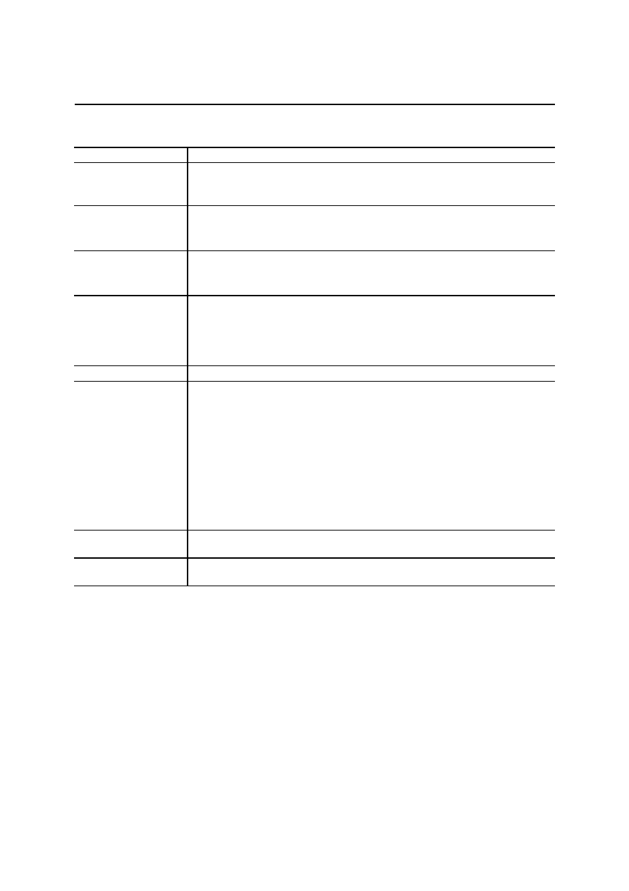
Symbol
Description
CSR
The input pin to select the transfer direction of the common signal output data.
At 1/n duty, data is transferred from COM1 to COMn when “L” is applied to this pin and
transferred from COMn to COM1 when “H” is applied to this pin.
SSR
The input pin to select the transfer direction of the segment signal output data.
“L”: Data transfer from SEG
1 to SEG100
“H”: Data transfer from SEG
100 to SEG1
V
1 , V2, V3A, V3B, V4
The pins to output bias voltages to the LCD.
For 1/4 bias : The V
2 and V3B pins are shorted.
For 1/5 bias : The V
3A and V3B pins are shorted.
BE
The input pin to enable or disable the voltage multiplier circuit.
"L" disables the voltage multiplier circuit. "H" enables the voltage multiplier circuit.
The voltage multiplier circuit doubles the input voltage between V
DD and VIN and the
multiplied voltage referenced to V
DD is output to the V5IN pin. The voltage multiplier
circuit can be used only when generating a level lower than GND.
V
IN
The pin to input voltage to the voltage multiplier.
V
5, V5IN
The pins to supply the LCD drive voltage.
The LCD drive voltage is supplied to the V
5 pin when the voltage multiplier is not used
(BE = “0”) and the internal contrast adjusting circuit is also not used. At this time, the
V
5IN pin should be open.
The LCD drive voltage is supplied to the V
5IN pin when the voltage multiplier is not used
(BE = “0”) but the internal contrast adjusting circuit is used. At this time, the V
5 pin
should be open.
When the voltage multiplier is used (BE = “1”), the V
5 pin should be open (the
multiplied voltage is output to the V
5IN pin). In this case, the internal contrast adjusting
circuit must be used. Capacitors for the voltage multiplier should be connected
between the V
DD pin and the V5IN pin.
V
C
The pin to connect the positive pin of the capacitor for the voltage multiplier. Leave the
pin open when the voltage multiplier circuit is not used.
V
CC
The pin to connect the negative pin of the capacitor used for the voltage multiplier.
Leave the pin open when the voltage multiplier circuit is not used.
相關(guān)PDF資料 |
PDF描述 |
|---|---|
| ML9042-01DVWA | 17 X 100 DOTS DOT MAT LCD DRVR AND DSPL CTLR, UUC233 |
| ML9042-01CVWA | 17 X 100 DOTS DOT MAT LCD DRVR AND DSPL CTLR, UUC233 |
| ML9042-01DVWA | 17 X 100 DOTS DOT MAT LCD DRVR AND DSPL CTLR, UUC233 |
| ML9042-11DVWA | 17 X 100 DOTS DOT MAT LCD DRVR AND DSPL CTLR, UUC233 |
| ML9042-21CVWA | 17 X 100 DOTS DOT MAT LCD DRVR AND DSPL CTLR, UUC233 |
相關(guān)代理商/技術(shù)參數(shù) |
參數(shù)描述 |
|---|---|
| ML9042 | 制造商:OKI 制造商全稱:OKI electronic componets 功能描述:DOT MATRIX LCD CONTROLLER DRIVER |
| ML9042-54CVWA-5016 | 制造商:ROHM Semiconductor 功能描述:RHOML9042-54CVWA-5016 OKI LCD DRIVER |
| ML9044 | 制造商:OKI 制造商全稱:OKI electronic componets 功能描述:DOT MATRIX LCD CONTROLLER DRIVER |
| ML9044A | 制造商:OKI 制造商全稱:OKI electronic componets 功能描述:DOT MATRIX LCD CONTROLLER DRIVER |
| ML9044A-XXACVWA | 制造商:OKI 制造商全稱:OKI electronic componets 功能描述:DOT MATRIX LCD CONTROLLER DRIVER |
發(fā)布緊急采購,3分鐘左右您將得到回復(fù)。