- 您現(xiàn)在的位置:買賣IC網(wǎng) > PDF目錄45333 > ML9041A-XXBCVWA (OKI ELECTRIC INDUSTRY CO LTD) 17 X 100 DOTS DOT MAT LCD DRVR AND DSPL CTLR, UUC175 PDF資料下載
參數(shù)資料
| 型號(hào): | ML9041A-XXBCVWA |
| 廠商: | OKI ELECTRIC INDUSTRY CO LTD |
| 元件分類: | 顯示控制器 |
| 英文描述: | 17 X 100 DOTS DOT MAT LCD DRVR AND DSPL CTLR, UUC175 |
| 封裝: | 10.62 X 2.55 MM, GOLD BUMP, DIE-175 |
| 文件頁(yè)數(shù): | 64/64頁(yè) |
| 文件大?。?/td> | 653K |
| 代理商: | ML9041A-XXBCVWA |
第1頁(yè)第2頁(yè)第3頁(yè)第4頁(yè)第5頁(yè)第6頁(yè)第7頁(yè)第8頁(yè)第9頁(yè)第10頁(yè)第11頁(yè)第12頁(yè)第13頁(yè)第14頁(yè)第15頁(yè)第16頁(yè)第17頁(yè)第18頁(yè)第19頁(yè)第20頁(yè)第21頁(yè)第22頁(yè)第23頁(yè)第24頁(yè)第25頁(yè)第26頁(yè)第27頁(yè)第28頁(yè)第29頁(yè)第30頁(yè)第31頁(yè)第32頁(yè)第33頁(yè)第34頁(yè)第35頁(yè)第36頁(yè)第37頁(yè)第38頁(yè)第39頁(yè)第40頁(yè)第41頁(yè)第42頁(yè)第43頁(yè)第44頁(yè)第45頁(yè)第46頁(yè)第47頁(yè)第48頁(yè)第49頁(yè)第50頁(yè)第51頁(yè)第52頁(yè)第53頁(yè)第54頁(yè)第55頁(yè)第56頁(yè)第57頁(yè)第58頁(yè)第59頁(yè)第60頁(yè)第61頁(yè)第62頁(yè)第63頁(yè)當(dāng)前第64頁(yè)
PEDL9041A-02
OKI Semiconductor
ML9041A-xxA/xxB
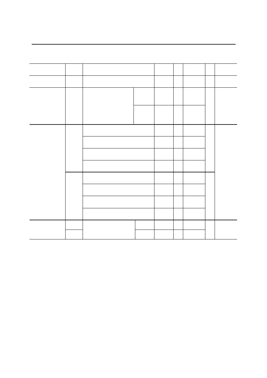
9/64
(GND = 0 V, V
DD = 2.7 to 5.5 V, Ta = –40 to +85°C)
Parameter
Symbol
Condition
Min.
Typ.
Max.
Unit
Applicable
pins
Voltage Multiplier
Input Voltage
V
MUL
Note 7
2.7
—
3.5
V
DD–VIN
1/5 bias
4.1
—
(V
DD–VIN)
× 2
Voltage Multiplier
Output Voltage
V
5OUT
V
DD = 2.7 V, VIN = 0 V
f = 125 kHz
A capacitor for the voltage
multiplier = 1 to 4.7
F
No load
BE = “H”
1/4 bias
3.9
—
(V
DD–VIN)
× 2
VV
DD–V5IN
V
DD =
5 V, V
5IN =
–2 V, 1/5 bias,
Contrast data: 1F, No load
6.6
—
V
DD =
5 V, V
5IN =
–2 V, 1/4 bias,
Contrast data: 1F, No load
6.6
—
V
DD =
4.1 V, V
5IN =
0 V, 1/5 bias,
Contrast data: 1F, No load
3.8
—
V
LCD
MAX
V
DD =
3.9 V, V
5IN =
0 V, 1/4 bias,
Contrast data: 1F, No load
3.6
—
V
DD =
5 V, V
5IN =
–2 V, 1/5 bias,
Contrast data: 00, No load
4.0
—
4.6
V
DD =
5 V, V
5IN =
–2 V, 1/4 bias,
Contrast data: 00, No load
3.6
—
4.2
V
DD =
4.1 V, V
5IN =
0 V, 1/5 bias,
Contrast data: 00, No load
2.2
—
2.8
Maximum and
minimum LCD
drive voltages
when internal
variable resistors
are used. Note 8
V
LCD
MIN
V
DD =
3.9 V, V
5IN =
0 V, 1/4 bias,
Contrast data: 00, No load
1.9
—
2.5
V
DD–V5
V
LCD1
1/5 bias
3.3
—
7.0
Bias Voltage for
Driving LCD
V
LCD2
V
DD–V5
Note 9
1/4 bias
3.3
—
7.0
VV
5
Note 1:
Applied to the voltage drop occurring between any of the V
DD, V1, V4 and V5 pins and any of the
common pins (COM
1 to COM17) when the current of 4 A flows in or flows out at one common
pin.
Also applied to the voltage drop occurring between any of the V
DD, V2, V3A (V3B) and V5 pins and
any of the segment pins (SEG
1 to SEG100) when the current of 4 A flows in or flows out at one
common pin.
The current of 4
A flows out when the output level is V
DD or flows in when the output level is
V
5.
Note 2:
Applied to the current flowing into the V
DD pin when the external clock (fOSC2 = fin = 270 kHz) is
fed to the internal R
f oscillation or OSC1 under the following conditions:
V
DD = 5 V
GND = V
5 = 0 V,
V
1, V2, V3A (V3B) and V4: Open
E, SSR, CSR, and BE: “L” (fixed)
Other input pins: “L” or “H” (fixed)
Other output pins: No load
相關(guān)PDF資料 |
PDF描述 |
|---|---|
| ML9042-01DVWA | 17 X 100 DOTS DOT MAT LCD DRVR AND DSPL CTLR, UUC233 |
| ML9042-01CVWA | 17 X 100 DOTS DOT MAT LCD DRVR AND DSPL CTLR, UUC233 |
| ML9042-01DVWA | 17 X 100 DOTS DOT MAT LCD DRVR AND DSPL CTLR, UUC233 |
| ML9042-11DVWA | 17 X 100 DOTS DOT MAT LCD DRVR AND DSPL CTLR, UUC233 |
| ML9042-21CVWA | 17 X 100 DOTS DOT MAT LCD DRVR AND DSPL CTLR, UUC233 |
相關(guān)代理商/技術(shù)參數(shù) |
參數(shù)描述 |
|---|---|
| ML9042 | 制造商:OKI 制造商全稱:OKI electronic componets 功能描述:DOT MATRIX LCD CONTROLLER DRIVER |
| ML9042-54CVWA-5016 | 制造商:ROHM Semiconductor 功能描述:RHOML9042-54CVWA-5016 OKI LCD DRIVER |
| ML9044 | 制造商:OKI 制造商全稱:OKI electronic componets 功能描述:DOT MATRIX LCD CONTROLLER DRIVER |
| ML9044A | 制造商:OKI 制造商全稱:OKI electronic componets 功能描述:DOT MATRIX LCD CONTROLLER DRIVER |
| ML9044A-XXACVWA | 制造商:OKI 制造商全稱:OKI electronic componets 功能描述:DOT MATRIX LCD CONTROLLER DRIVER |
發(fā)布緊急采購(gòu),3分鐘左右您將得到回復(fù)。