- 您現(xiàn)在的位置:買賣IC網(wǎng) > PDF目錄224391 > MPC104AU (TEXAS INSTRUMENTS INC) 2-CHANNEL, VIDEO MULTIPLEXER, PDSO8 PDF資料下載
參數(shù)資料
| 型號: | MPC104AU |
| 廠商: | TEXAS INSTRUMENTS INC |
| 元件分類: | 多路復(fù)用及模擬開關(guān) |
| 英文描述: | 2-CHANNEL, VIDEO MULTIPLEXER, PDSO8 |
| 封裝: | SO-8 |
| 文件頁數(shù): | 2/16頁 |
| 文件大?。?/td> | 172K |
| 代理商: | MPC104AU |
MPC104
10
quired to avoid synchronization by large negative output
glitches in subsequent equipment.
The SEL-to-channel-ON time is typically 25ns and always
shorter than the typical SEL-to-channel-OFF time of 250ns.
In the worst case, an ON/OFF margin of 150ns ensures safe
switching even for timing spreads in the digital control
latches. The short interchannel switching time of 300ns
allows channel change during the vertical blanking time,
even in high-resolution graphic or broadcast systems. As
shown in the typical performance curves, the signal enve-
lope during transition from one channel to another rises and
falls symmetrically and shows less overshooting and DC
settling effects.
Power consumption is a serious problem when designing
large crosspoint fields with high component density. Most of
the buffer amplifiers are in the off-state. One important
design goal was to attain low off-state quiescent current
when no channel is selected. The low supply current of
±120A when no channel is selected and ±4.6mA when one
channel is selected, as well as the reduced
±5V supply
voltage, conserves power, simplifies the power supply de-
sign, and results in cooler, more reliable operation.
CIRCUIT LAYOUT
The high-frequency performance of the MPC104 can be
greatly affected by the physical layout of the circuit. The
following tips are offered as suggestions, not as absolutes.
Oscillations, ringing, poor bandwidth and settling, higher
crosstalk, and peaking are all typical problems which plague
high-speed components when they are used incorrectly.
Bypass power supplies very close to the device pins. Use
tantalum chip capacitors (approximately 2.2
F), a parallel
470pF ceramic chip capacitor may be added if desired.
Surface-mount types are recommended due to their low
lead inductance.
PC board traces for signal and power lines should be wide
to reduce impedance or inductance.
Make short and low inductance traces. The entire physical
circuit should be as small as possible.
Use a low-impedance ground plane on the component side
to ensure that low-impedance ground is available through-
out the layout. Grounded traces between the input traces
are essential to achieve high interchannel crosstalk rejec-
tion.
Do not extend the ground plane under high-impedance
nodes sensitive to stray capacitances, such as the buffer’s
input terminals.
Sockets are not recommended, because they add signifi-
cant inductance and parasitic capacitance. If sockets must
be used, consider using zero-profile solderless sockets.
Use low-inductance and surface-mounted components.
Circuits using all surface mount components with the
MPC104 will offer the best AC-performance.
A resistor (100
to 150) in series with the input of the
buffers may help to reduce peaking. Place the resistor as
close as possible to the pin.
Plug-in prototype boards and wire-wrap boards will not
function well. A clean layout using RF techniques is
essential—there are no shortcuts.
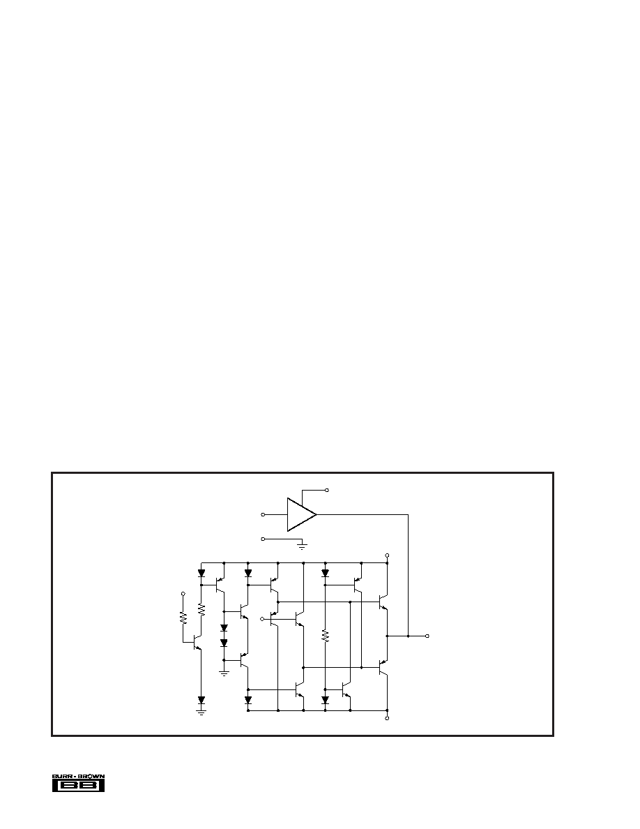
FIGURE 2. Simplified Circuit Diagram.
IN
2
+V
CC = +5V
V
OUT
(4)
DB2
(6)
–V
CC = –5V
(3)
(7)
(5)
SEL
2
DB1
(8)
(1)
(2)
IN
1
GND
SEL
1
相關(guān)PDF資料 |
PDF描述 |
|---|---|
| MPC308-725C | SIP8, IC SOCKET |
| MPC624-726C | SIP24, IC SOCKET |
| MPC628-710C | SIP28, IC SOCKET |
| MPC314-710C | SIP14, IC SOCKET |
| MPC314-726C | SIP14, IC SOCKET |
相關(guān)代理商/技術(shù)參數(shù) |
參數(shù)描述 |
|---|---|
| MPC104G100 | 制造商:FDYNE 功能描述:AF410X100 2% |
| MPC-104G100 | 制造商:FDYNE 功能描述:AF410X100 2% |
| MPC1055L1R0C | 制造商:KEMET Corporation 功能描述: 制造商:KEMET Corporation 功能描述:INDUCTOR POWER 1UH 20% SMD - Tape and Reel 制造商:KEMET Corporation 功能描述:Fixed Inductors 1uH 20% SMD |
| MPC1055LR36C | 制造商:KEMET Corporation 功能描述: 制造商:KEMET Corporation 功能描述:INDUCTOR POWER 0.36UH 20% SMD - Tape and Reel 制造商:NEC TOKIN Corporation 功能描述:MPC Series 0.36uH 20% Unshielded SMD Power Inductor 制造商:KEMET Corporation 功能描述:Fixed Inductors 0.36uH 20% SMD |
| MPC106 | 制造商:MOTOROLA 制造商全稱:Motorola, Inc 功能描述:PCI Bridge/Memory Controller |
發(fā)布緊急采購,3分鐘左右您將得到回復(fù)。