- 您現(xiàn)在的位置:買賣IC網(wǎng) > PDF目錄67997 > MPC5606SVMG6R (FREESCALE SEMICONDUCTOR INC) 32-BIT, FLASH, 64 MHz, MICROCONTROLLER, PBGA208 PDF資料下載
參數(shù)資料
| 型號(hào): | MPC5606SVMG6R |
| 廠商: | FREESCALE SEMICONDUCTOR INC |
| 元件分類: | 微控制器/微處理器 |
| 英文描述: | 32-BIT, FLASH, 64 MHz, MICROCONTROLLER, PBGA208 |
| 封裝: | 17 X 17 MM, 1 MM PITCH, MAPBGA-208 |
| 文件頁數(shù): | 83/134頁 |
| 文件大小: | 890K |
| 代理商: | MPC5606SVMG6R |
第1頁第2頁第3頁第4頁第5頁第6頁第7頁第8頁第9頁第10頁第11頁第12頁第13頁第14頁第15頁第16頁第17頁第18頁第19頁第20頁第21頁第22頁第23頁第24頁第25頁第26頁第27頁第28頁第29頁第30頁第31頁第32頁第33頁第34頁第35頁第36頁第37頁第38頁第39頁第40頁第41頁第42頁第43頁第44頁第45頁第46頁第47頁第48頁第49頁第50頁第51頁第52頁第53頁第54頁第55頁第56頁第57頁第58頁第59頁第60頁第61頁第62頁第63頁第64頁第65頁第66頁第67頁第68頁第69頁第70頁第71頁第72頁第73頁第74頁第75頁第76頁第77頁第78頁第79頁第80頁第81頁第82頁當(dāng)前第83頁第84頁第85頁第86頁第87頁第88頁第89頁第90頁第91頁第92頁第93頁第94頁第95頁第96頁第97頁第98頁第99頁第100頁第101頁第102頁第103頁第104頁第105頁第106頁第107頁第108頁第109頁第110頁第111頁第112頁第113頁第114頁第115頁第116頁第117頁第118頁第119頁第120頁第121頁第122頁第123頁第124頁第125頁第126頁第127頁第128頁第129頁第130頁第131頁第132頁第133頁第134頁
MPC560xS Microcontroller Data Sheet, Rev. 5
Preliminary—Subject to Change Without Notice
Pinout and signal descriptions
Freescale Semiconductor
52
2.9.1
Signal details
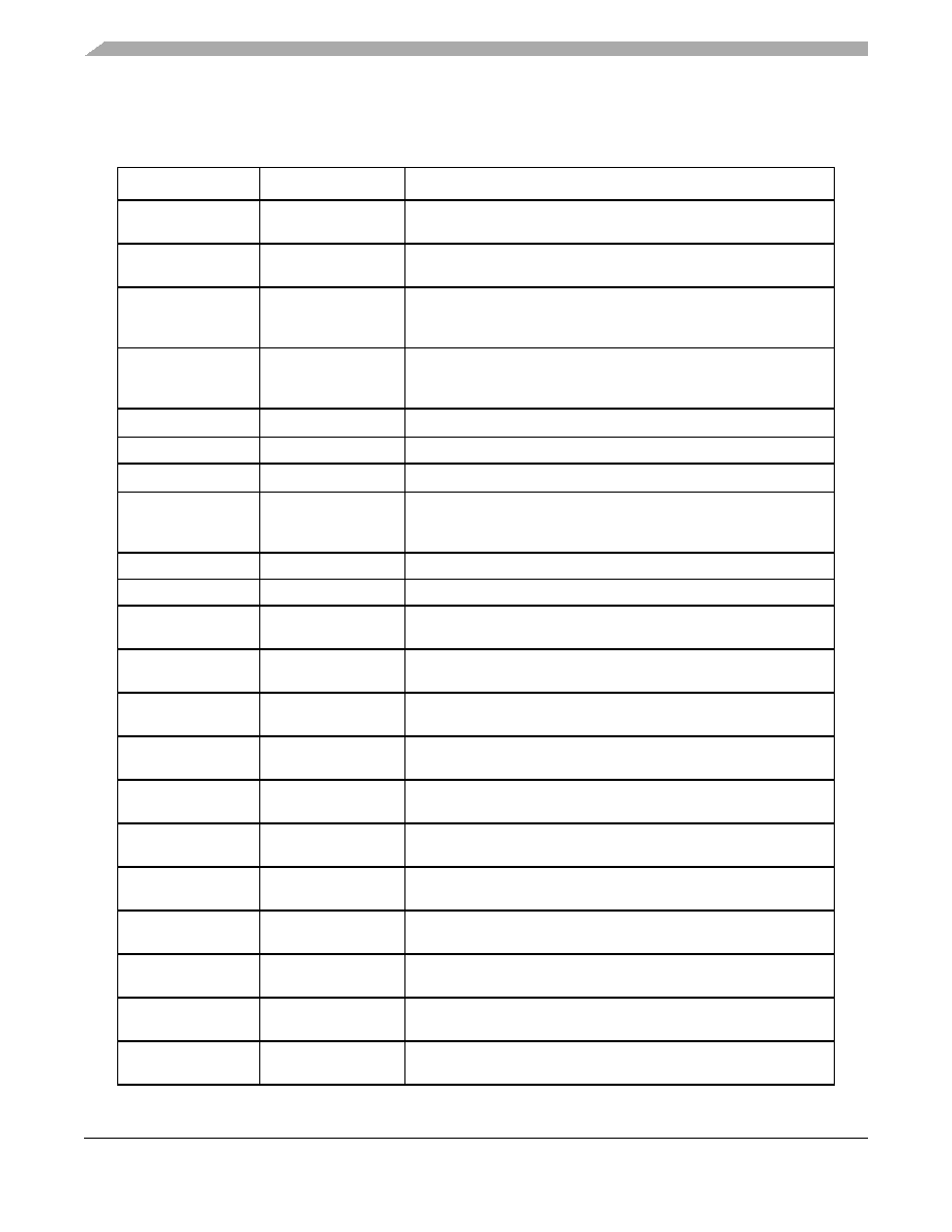
Table 10. Signal details
Signal
Peripheral
Description
ABS[0]
BAM
Alternate Boot Select. Gives an option to boot by downloading code
via CAN or LIN.
ANS[0:15]
ADC
Inputs used to bring into the device sensor-based signals for A/D
conversion. ANS[0:15] connect to ATD channels [32:47].
MA[0:2]
ADC
These three control bits are output to enable the selection for an
external Analog Mux for expansion channels. The available 8
multiplexed channels connect to ATD channels [64:71].
FABM
Force Alternate Boot mode. Forces the device to boot from the
external bus (Can or LIN). If not asserted, the device boots up from
the lowest flash sector containing a valid boot signature.
DCU_DE
DCU
Indicates that valid pixels are present.
DCU_HSYNC
DCU
Horizontal sync pulse for TFT-LCD display
DCU_PCLK
DCU
Output pixel clock for TFT-LCD display
DCU_R[0:7],
DCU_G[0:7],
DCU_B[0:7]
DCU
Red, green and blue color 8-bit Pixel values for TFT-LCD displays
DCU_TAG
DCU
Indicates when a tagged pixel is present in safety mode
DCU_VSYNC
DCU
Vertical sync pulse for TFT-LCD display
PCS[0..2]_0,
PCS[0..2]_1
DSPI
Peripheral chip selects when device is in Master mode; not used in
slave modes.
SCK_0,
SCK_1
DSPI
SPI clock signal—bidirectional
SIN_0,
SIN_1
DSPI
SPI data input signal
SOUT_0,
SOUT_1
DSPI
SPI data output signal
PCS0_2
QuadSPI
Peripheral chip select for serial flash mode or chip select 0 for SPI
master mode
IO2/PCS1_2
QuadSPI
Chip select 1 for SPI master mode and bidirectional IO2 for serial
flash mode
IO3/PCS2_2
QuadSPI
Chip select 2 for SPI master mode and bidirectional IO3 for serial
flash mode
IO0/SIN_2
QuadSPI
Data input signal for SPI master and slave modes and bidirectional
IO0 for serial flash mode
IO1/SOUT_2
QuadSPI
Data output signal for SPI master and slave modes and bidirectional
IO1 for serial flash mode
SCK_2
QuadSPI
Clock output signal for SPI master and serial flash modes and clock
input signal for SPI slave mode
eMIOSA[8:23],
eMIOSB[16:23]
eMIOS
Enhanced Modular Input Output System. 16+8 channel eMIOS for
timed input or output functions.
Because
of
an
order
from
the
United
States
International
Trade
Commission,
BGA-packaged
product
lines
and
part
numbers
indicated
here
currently
are
not
available
from
Freescale
for
import
or
sale
in
the
United
States
prior
to
September
2010:
MPC5606S
products
in
208
MAPBGA
packages
相關(guān)PDF資料 |
PDF描述 |
|---|---|
| MPC5606SCMG6 | 32-BIT, FLASH, 64 MHz, MICROCONTROLLER, PBGA208 |
| MPC602AFUXXEX | RISC PROCESSOR, PQFP144 |
| MPC602AFUXXCX | RISC PROCESSOR, PQFP144 |
| MPC603PRX166LX | 32-BIT, 166 MHz, RISC PROCESSOR, CBGA255 |
| MPC603PRX180LX | 32-BIT, 180 MHz, RISC PROCESSOR, CBGA255 |
相關(guān)代理商/技術(shù)參數(shù) |
參數(shù)描述 |
|---|---|
| MPC5607B | 制造商:Freescale Semiconductor 功能描述: |
| MPC5607B_13 | 制造商:FREESCALE 制造商全稱:Freescale Semiconductor, Inc 功能描述:MicrocontrollerData Sheet |
| MPC5607BECLLR | 制造商:FREESCALE 制造商全稱:Freescale Semiconductor, Inc 功能描述:Microcontroller |
| MPC5607BECLQR | 制造商:FREESCALE 制造商全稱:Freescale Semiconductor, Inc 功能描述:Microcontroller |
| MPC5607BECLUR | 制造商:FREESCALE 制造商全稱:Freescale Semiconductor, Inc 功能描述:Microcontroller |
發(fā)布緊急采購,3分鐘左右您將得到回復(fù)。