- 您現(xiàn)在的位置:買賣IC網(wǎng) > PDF目錄371136 > MPIC2131 (Motorola, Inc.) 3 HIGH SIDE & 3 LOW SIDE DRIVER PDF資料下載
參數(shù)資料
| 型號: | MPIC2131 |
| 廠商: | Motorola, Inc. |
| 英文描述: | 3 HIGH SIDE & 3 LOW SIDE DRIVER |
| 中文描述: | 3高壓側(cè) |
| 文件頁數(shù): | 1/6頁 |
| 文件大?。?/td> | 172K |
| 代理商: | MPIC2131 |

1
Motorola, Inc. 1996
Power Products Division
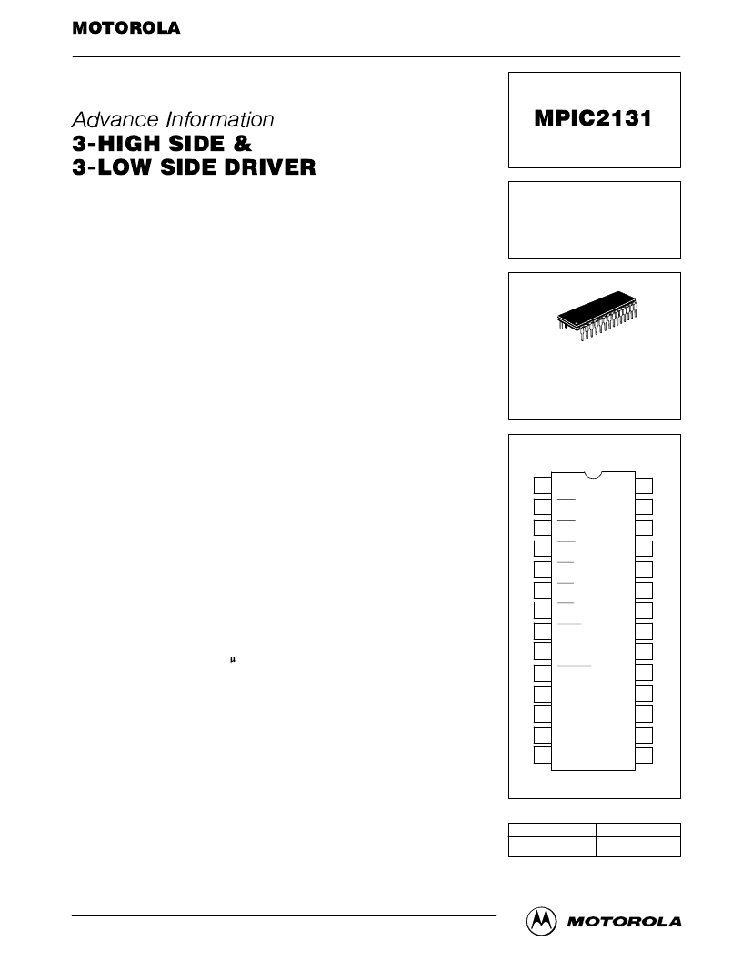
The MPIC2131 is a high voltage, high speed, power MOSFET and IGBT driver
with three independent high side and low side referenced output channels for
3–Phase applications. Proprietary HVIC technology enables ruggedized monolith-
ic construction. Logic inputs are compatible with 5 V CMOS or LSTTL outputs. A
ground referenced operational amplifier provides an analog feedback of bridge
current via an external current sense resistor. A current trip function which termi-
nates all six outputs is also derived from an external current sense resistor. An ex-
tra shutdown input is provided for customizing the shutdown function. An open
drain FAULT signal is provided to indicate that any of shutdown conditions has oc-
curred. The output drivers feature a high pulse current buffer stage designed for
minimum driver cross–conduction. Propagation delays are matched to simplify use
in high frequency applications.
The floating channels can be used to drive N–channel power MOSFET or
IGBT’s in the high side configuration which operate from 10 to 600 volts.
Floating Channel Designed for Bootstrap Operation
Fully Operational to +600 V
Tolerant to Negative Transient Voltage
dV/dt Immune
Gate Drive Supply Range from 10 to 20 V
Undervoltage Lockout for All Channels
Over–current Shut Down Turns Off All Six Drivers
Independent 3 High Side & 3 Low Side Drivers
Matched Propagation Delay for All Channels
Outputs Out of Phase with Inputs
PRODUCT SUMMARY
600 V MAX
200 mA/420 mA
10 – 20 V
1.4 & 0.7 s
700 ns
VOFFSET
IO+/–
VOUT
ton/off (typical)
Delay Matching
This document contains information on a new product. Specifications and information herein are subject
to change without notice.
REV 1
Order this document
by MPIC2131/D
SEMICONDUCTOR TECHNICAL DATA
Device
MPIC2131P
Package
PDIP
3 HIGH SIDE &
3 LOW SIDE
DRIVER
ORDERING INFORMATION
(TOP VIEW)
PIN CONNECTIONS
P SUFFIX
PLASTIC PACKAGE
CASE 710–02
28
1
1
2
3
4
5
6
7
8
22
23
24
25
26
27
28
9
21
20
10
11
12
13
14
17
18
19
16
15
VCC
HIN1
HIN2
HIN3
LIN1
LIN2
LIN3
FAULT
ITRIP
FLT+CLR
SD
VSS
COM
LO3
VB1
HO1
VS1
VB2
HO2
VS2
VB3
HO3
VS3
LO1
LO2
相關(guān)PDF資料 |
PDF描述 |
|---|---|
| MPIC2131P | 3 HIGH SIDE & 3 LOW SIDE DRIVER |
| MPQ6001N | QUAD DUAL IN LINE SILICON COMPLEMENTARY PAIR TRANSISTORS |
| MPQ6001 | QUAD DUAL IN LINE SILICON COMPLEMENTARY PAIR TRANSISTORS |
| MPQ6002N | QUAD DUAL IN LINE SILICON COMPLEMENTARY PAIR TRANSISTORS |
| MPQ6501 | QUAD DUAL IN LINE SILICON COMPLEMENTARY PAIR TRANSISTORS |
相關(guān)代理商/技術(shù)參數(shù) |
參數(shù)描述 |
|---|---|
| MPIC2131P | 制造商:MOTOROLA 制造商全稱:Motorola, Inc 功能描述:3 HIGH SIDE & 3 LOW SIDE DRIVER |
| MPIC2151 | 制造商:MOTOROLA 制造商全稱:Motorola, Inc 功能描述:SELF-OSCILLATING HALF-BRIDGE DRIVER |
| MPIC5060 | 制造商:Electronic Devices, Inc. 功能描述:MiniBridge, 600 volt, Bulk |
| MPIL | 制造商:EDI 制造商全稱:Electronic devices inc. 功能描述:40/50 AMPERE SINGLE-PHASE, FULL-WAVE BRIDGES |
| MPIL05 | 制造商:EDI 制造商全稱:Electronic devices inc. 功能描述:40/50 AMPERE SINGLE-PHASE, FULL-WAVE BRIDGES |
發(fā)布緊急采購,3分鐘左右您將得到回復(fù)。