- 您現(xiàn)在的位置:買賣IC網(wǎng) > PDF目錄25627 > MQ80C52XXX-36/883:RD (ATMEL CORP) 8-BIT, MROM, 36 MHz, MICROCONTROLLER, CQFP44 PDF資料下載
參數(shù)資料
| 型號: | MQ80C52XXX-36/883:RD |
| 廠商: | ATMEL CORP |
| 元件分類: | 微控制器/微處理器 |
| 英文描述: | 8-BIT, MROM, 36 MHz, MICROCONTROLLER, CQFP44 |
| 封裝: | CERAMIC, QFP-44 |
| 文件頁數(shù): | 21/28頁 |
| 文件大小: | 6193K |
第1頁第2頁第3頁第4頁第5頁第6頁第7頁第8頁第9頁第10頁第11頁第12頁第13頁第14頁第15頁第16頁第17頁第18頁第19頁第20頁當前第21頁第22頁第23頁第24頁第25頁第26頁第27頁第28頁

28
2467X–AVR–06/11
ATmega128
Pull-up and Bus-
keeper
The pull-ups on the AD7:0 ports may be activated if the corresponding Port register is written to
one. To reduce power consumption in sleep mode, it is recommended to disable the pull-ups by
writing the Port register to zero before entering sleep.
The XMEM interface also provides a bus-keeper on the AD7:0 lines. The bus-keeper can be dis-
abled and enabled in software as described in “External Memory Control Register B – XMCRB”
on page 32. When enabled, the bus-keeper will ensure a defined logic level (zero or one) on the
AD7:0 bus when these lines would otherwise be tri-stated by the XMEM interface.
Timing
External Memory devices have different timing requirements. To meet these requirements, the
ATmega128 XMEM interface provides four different wait-states as shown in Table 4. It is impor-
tant to consider the timing specification of the External Memory device before selecting the wait-
state. The most important parameters are the access time for the external memory compared to
the set-up requirement of the ATmega128. The access time for the External Memory is defined
to be the time from receiving the chip select/address until the data of this address actually is
driven on the bus. The access time cannot exceed the time from the ALE pulse must be
asserted low until data is stable during a read sequence (See t
additional feature, it is possible to divide the external memory space in two sectors with individ-
ual wait-state settings. This makes it possible to connect two different memory devices with
different timing requirements to the same XMEM interface. For XMEM interface timing details,
Note that the XMEM interface is asynchronous and that the waveforms in the following figures
are related to the internal system clock. The skew between the internal and external clock
(XTAL1) is not guarantied (varies between devices temperature, and supply voltage). Conse-
quently, the XMEM interface is not suited for synchronous operation.
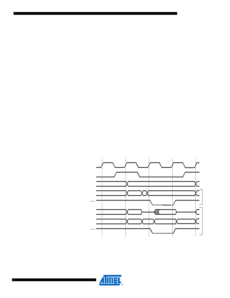
Figure 13. External Data Memory Cycles without Wait-state (SRWn1=0 and SRWn0=0)
Note:
1. SRWn1 = SRW11 (upper sector) or SRW01 (lower sector), SRWn0 = SRW10 (upper sector) or
SRW00 (lower sector). The ALE pulse in period T4 is only present if the next instruction
accesses the RAM (internal or external).
ALE
T1
T2
T3
W
rite
Read
WR
T4
A15:8
Address
Prev. addr.
DA7:0
Address
Data
Prev. data
XX
RD
DA7:0 (XMBK = 0)
Data
Prev. data
Address
Data
Prev. data
Address
DA7:0 (XMBK = 1)
System Clock (CLKCPU)
XXXXX
XXXXXXXX
相關(guān)PDF資料 |
PDF描述 |
|---|---|
| MD80C32E-16SHXXX:D | 8-BIT, 16 MHz, MICROCONTROLLER, CDIP40 |
| MR83C154XXX-16P883D | 8-BIT, MROM, 16 MHz, MICROCONTROLLER, CQCC44 |
| MR80C52XXX-30/883:RD | 8-BIT, MROM, 30 MHz, MICROCONTROLLER, CQCC44 |
| MQ80C32-36/883R | 8-BIT, 36 MHz, MICROCONTROLLER, CQFP44 |
| MD83C154DXXX-12/883 | 8-BIT, MROM, 12 MHz, MICROCONTROLLER, CDIP40 |
相關(guān)代理商/技術(shù)參數(shù) |
參數(shù)描述 |
|---|---|
| MQ82370-20 | 制造商:Rochester Electronics LLC 功能描述:- Bulk |
| MQ8238020 | 制造商:Intel 功能描述:CONTROLLER: OTHER |
| MQ82380-20 | 制造商:Rochester Electronics LLC 功能描述:- Bulk |
| MQ82380-20/R | 制造商:Rochester Electronics LLC 功能描述: |
| MQ82592 | 制造商:Rochester Electronics LLC 功能描述:- Bulk |
發(fā)布緊急采購,3分鐘左右您將得到回復(fù)。