- 您現(xiàn)在的位置:買賣IC網 > PDF目錄25637 > MR83C154XXX-25/883D (ATMEL CORP) 8-BIT, MROM, 25 MHz, MICROCONTROLLER, CQCC44 PDF資料下載
參數資料
| 型號: | MR83C154XXX-25/883D |
| 廠商: | ATMEL CORP |
| 元件分類: | 微控制器/微處理器 |
| 英文描述: | 8-BIT, MROM, 25 MHz, MICROCONTROLLER, CQCC44 |
| 封裝: | LCC-44 |
| 文件頁數: | 20/141頁 |
| 文件大小: | 7628K |
| 代理商: | MR83C154XXX-25/883D |
第1頁第2頁第3頁第4頁第5頁第6頁第7頁第8頁第9頁第10頁第11頁第12頁第13頁第14頁第15頁第16頁第17頁第18頁第19頁當前第20頁第21頁第22頁第23頁第24頁第25頁第26頁第27頁第28頁第29頁第30頁第31頁第32頁第33頁第34頁第35頁第36頁第37頁第38頁第39頁第40頁第41頁第42頁第43頁第44頁第45頁第46頁第47頁第48頁第49頁第50頁第51頁第52頁第53頁第54頁第55頁第56頁第57頁第58頁第59頁第60頁第61頁第62頁第63頁第64頁第65頁第66頁第67頁第68頁第69頁第70頁第71頁第72頁第73頁第74頁第75頁第76頁第77頁第78頁第79頁第80頁第81頁第82頁第83頁第84頁第85頁第86頁第87頁第88頁第89頁第90頁第91頁第92頁第93頁第94頁第95頁第96頁第97頁第98頁第99頁第100頁第101頁第102頁第103頁第104頁第105頁第106頁第107頁第108頁第109頁第110頁第111頁第112頁第113頁第114頁第115頁第116頁第117頁第118頁第119頁第120頁第121頁第122頁第123頁第124頁第125頁第126頁第127頁第128頁第129頁第130頁第131頁第132頁第133頁第134頁第135頁第136頁第137頁第138頁第139頁第140頁第141頁
200
8021G–AVR–03/11
ATmega329P/3290P
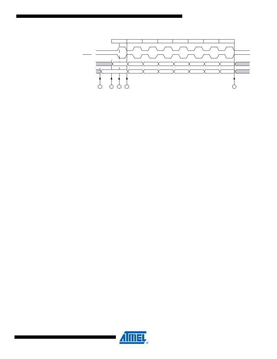
Figure 20-3. Three-wire Mode, Timing Diagram
The Three-wire mode timing is shown in Figure 20-3. At the top of the figure is a USCK cycle ref-
erence. One bit is shifted into the USI Shift Register (USIDR) for each of these cycles. The
USCK timing is shown for both external clock modes. In External Clock mode 0 (USICS0 = 0), DI
is sampled at positive edges, and DO is changed (Data Register is shifted by one) at negative
edges. External Clock mode 1 (USICS0 = 1) uses the opposite edges versus mode 0, i.e., sam-
ples data at negative and changes the output at positive edges. The USI clock modes
corresponds to the SPI data mode 0 and 1.
Referring to the timing diagram (Figure 20-3), a bus transfer involves the following steps:
1.
The Slave device and Master device sets up its data output and, depending on the proto-
col used, enables its output driver (mark A and B). The output is set up by writing the
data to be transmitted to the Serial Data Register. Enabling of the output is done by set-
ting the corresponding bit in the port Data Direction Register. Note that point A and B
does not have any specific order, but both must be at least one half USCK cycle before
point C where the data is sampled. This must be done to ensure that the data setup
requirement is satisfied. The 4-bit counter is reset to zero.
2.
The Master generates a clock pulse by software toggling the USCK line twice (C and D).
The bit value on the slave and master’s data input (DI) pin is sampled by the USI on the
first edge (C), and the data output is changed on the opposite edge (D). The 4-bit counter
will count both edges.
3.
Step 2. is repeated eight times for a complete register (byte) transfer.
4.
After eight clock pulses (i.e., 16 clock edges) the counter will overflow and indicate that
the transfer is completed. The data bytes transferred must now be processed before a
new transfer can be initiated. The overflow interrupt will wake up the processor if it is set
to Idle mode. Depending of the protocol used the slave device can now set its output to
high impedance.
20.3.2
SPI Master Operation Example
The following code demonstrates how to use the USI module as a SPI Master:
SPITransfer:
sts
USIDR,r16
ldi
r16,(1<<USIOIF)
sts
USISR,r16
ldi
r16,(1<<USIWM0)|(1<<USICS1)|(1<<USICLK)|(1<<USITC)
SPITransfer_loop:
sts
USICR,r16
lds
r16, USISR
sbrs
r16, USIOIF
MSB
654321
LSB
1
2
3
4
5
6
7
8
654321
LSB
USCK
DO
DI
D
C
B
A
E
CYCLE ( Reference )
相關PDF資料 |
PDF描述 |
|---|---|
| MD80C32E-16/883 | 8-BIT, 16 MHz, MICROCONTROLLER, CDIP40 |
| MC80C52EXXX-25/883:D | 8-BIT, MROM, 25 MHz, MICROCONTROLLER, CDIP40 |
| MR80C52EXXX-12/883:R | 8-BIT, MROM, 12 MHz, MICROCONTROLLER, CQCC44 |
| MC80C52XXX-16SHXXX:D | 8-BIT, MROM, 16 MHz, MICROCONTROLLER, CDIP40 |
| MQ80C52TXXX-30SBR | 8-BIT, MROM, 30 MHz, MICROCONTROLLER, CQFP44 |
相關代理商/技術參數 |
參數描述 |
|---|---|
| MR850 | 功能描述:整流器 3.0 Amp 50 Volt 150ns RoHS:否 制造商:Vishay Semiconductors 產品:Standard Recovery Rectifiers 配置: 反向電壓:100 V 正向電壓下降: 恢復時間:1.2 us 正向連續(xù)電流:2 A 最大浪涌電流:35 A 反向電流 IR:5 uA 安裝風格:SMD/SMT 封裝 / 箱體:DO-221AC 封裝:Reel |
| MR850 _AY _10001 | 制造商:PanJit Touch Screens 功能描述: |
| MR850 R0 | 制造商:SKMI/Taiwan 功能描述:Diode Switching 50V 3A 2-Pin DO-201AD T/R |
| MR850_ R2 _10001 | 制造商:PanJit Touch Screens 功能描述: |
| MR850_09 | 制造商:PANJIT 制造商全稱:Pan Jit International Inc. 功能描述:SOFT RECOVERY, FAST SWITCHING PLASTIC RECTIFIER |
發(fā)布緊急采購,3分鐘左右您將得到回復。