- 您現(xiàn)在的位置:買賣IC網(wǎng) > PDF目錄378017 > MSM7602-001 (OKI SEMICONDUCTOR CO., LTD.) Echo Canceler PDF資料下載
參數(shù)資料
| 型號: | MSM7602-001 |
| 廠商: | OKI SEMICONDUCTOR CO., LTD. |
| 英文描述: | Echo Canceler |
| 中文描述: | 回聲消除器 |
| 文件頁數(shù): | 12/29頁 |
| 文件大小: | 238K |
| 代理商: | MSM7602-001 |
第1頁第2頁第3頁第4頁第5頁第6頁第7頁第8頁第9頁第10頁第11頁當前第12頁第13頁第14頁第15頁第16頁第17頁第18頁第19頁第20頁第21頁第22頁第23頁第24頁第25頁第26頁第27頁第28頁第29頁
Semiconductor
MSM7602
12/29
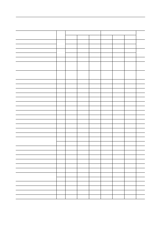
AC Characteristics
Parameter
Clock Frequency
When Internal Sync Signal is not used
Clock Cycle Time
When Internal Sync Signal is not used
Clock Duty Ratio
Clock "H" Level Pulse Width
fc = 19.2 MHz
Clock "L" Level Pulse Width
fc = 19.2 MHz
Clock Rise Time
Clock Fall Time
Sync Clock Output Time
Internal Sync Clock Frequency
Internal Sync Clock Output Cycle Time
Internal Sync Clock Duty Ratio
Internal Sync Signal Output Delay Time
Internal Sync Signal Period
Internal Sync Signal Output Width
Transmit/receive Operation Clock Frequency
Transmit/receive Sync Clock Cycle Time
Transmit/receive Sync Clock Duty Ratio
Transmit/receive Sync Signal Period
Sync Timing
Sync Signal Width
Receive Signal Setup Time
Receive Signal Hold Time
Receive Data Input Time
IRLD
Signal Output Delay Time
IRLD
Signal Output Width
Serial Output Delay Time
Symbol
f
C
t
MCK
t
DMC
t
MCH
t
MCL
t
r
t
f
t
DCM
f
CO
t
CO
t
DCO
t
DCC
t
CYO
t
WSO
f
SCK
t
SCK
t
DSC
t
CYC
t
XS
t
SX
t
WSY
t
DS
t
DH
t
ID
t
DIC
t
WIR
t
SD
t
XD
t
WR
t
DRS
t
DRE
t
DIT
Min.
—
17.5
—
50
40
20.8
20.8
—
—
—
—
—
—
64
0.488
40
123
45
45
t
SCK
45
45
—
—
—
—
—
1
5
—
Typ.
19.2
—
52.08
—
—
—
—
256
3.9
50
—
125
t
CO
—
—
50
125
—
—
—
—
—
7t
SCK
—
t
SCK
—
—
—
—
—
Max.
—
20
—
57.14
60
31.3
31.3
—
—
—
5
—
—
2048
15.6
60
—
—
t
CYC
-t
SCK
—
—
—
—
138
—
90
90
—
—
52
Min.
—
17.5
—
50
40
20.8
20.8
—
—
—
—
—
—
—
—
—
64
0.488
40
123
45
45
t
SCK
45
45
—
—
—
—
—
1
5
—
100
Typ.
19.2
—
52.08
—
—
—
—
—
—
—
256
3.9
50
—
125
t
CO
—
—
50
125
—
—
—
—
—
7t
SCK
—
t
SCK
—
—
—
—
—
—
Max.
—
20
—
57.14
60
31.3
31.3
5
5
30
—
—
—
5
—
—
2048
15.6
60
—
—
t
CYC
-t
SCK
—
—
—
—
138
—
90
90
—
—
52
—
Unit
MHz
ns
ns
ns
ns
ns
ns
ns
kHz
m
s
%
ns
m
s
m
s
kHz
m
s
%
m
s
ns
ns
m
s
ns
ns
m
s
ns
m
s
ns
ns
m
s
ns
ns
m
s
V
DD
= 2.7 V to 3.6 V
V
DD
= 4.5 V to 5.5 V
(Ta = –40C to +85C)
Reset Start Time
Reset End Time
Processing Operation Start Time
100
—
—
Reset Signal Input Width
—
—
30
—
—
5
—
—
5
相關(guān)PDF資料 |
PDF描述 |
|---|---|
| MSM7602-011 | Echo Canceler |
| MSM7603 | Echo Canceler |
| MSM7603B | Echo Canceler |
| MSM7630 | Universal Speech Processor(通用語音處理器) |
| MSM7661B | NTSC/PAL Digital Dencoder(NTSC/PAL制式數(shù)字譯碼器) |
相關(guān)代理商/技術(shù)參數(shù) |
參數(shù)描述 |
|---|---|
| MSM7602-001GS-K | 制造商:ROHM Semiconductor 功能描述: |
| MSM7602-011 | 制造商:OKI 制造商全稱:OKI electronic componets 功能描述:Echo Canceler |
| MSM7603 | 制造商:OKI 制造商全稱:OKI electronic componets 功能描述:Echo Canceler |
| MSM7603B | 制造商:OKI 制造商全稱:OKI electronic componets 功能描述:Echo Canceler |
| MSM7617 | 制造商:OKI 制造商全稱:OKI electronic componets 功能描述:2-Channel Echo Canceler |
發(fā)布緊急采購,3分鐘左右您將得到回復(fù)。