- 您現(xiàn)在的位置:買賣IC網(wǎng) > PDF目錄224505 > MT28C128564W18EBW-F605P706TBWT SPECIALTY MEMORY CIRCUIT, PBGA77 PDF資料下載
參數(shù)資料
| 型號: | MT28C128564W18EBW-F605P706TBWT |
| 元件分類: | 存儲器 |
| 英文描述: | SPECIALTY MEMORY CIRCUIT, PBGA77 |
| 封裝: | LEAD FREE, FBGA-77 |
| 文件頁數(shù): | 14/15頁 |
| 文件大小: | 203K |
| 代理商: | MT28C128564W18EBW-F605P706TBWT |
128Mb MULTIBANK BURST FLASH
32Mb/64Mb BURST CellularRAM COMBO
09005aef80df9a45
Micron Technology, Inc., reserves the right to change products or specifications without notice.
MT28C128564W18E.fm - Rev. C Pub 2/04 EN
8
2004 Micron Technology. Inc.
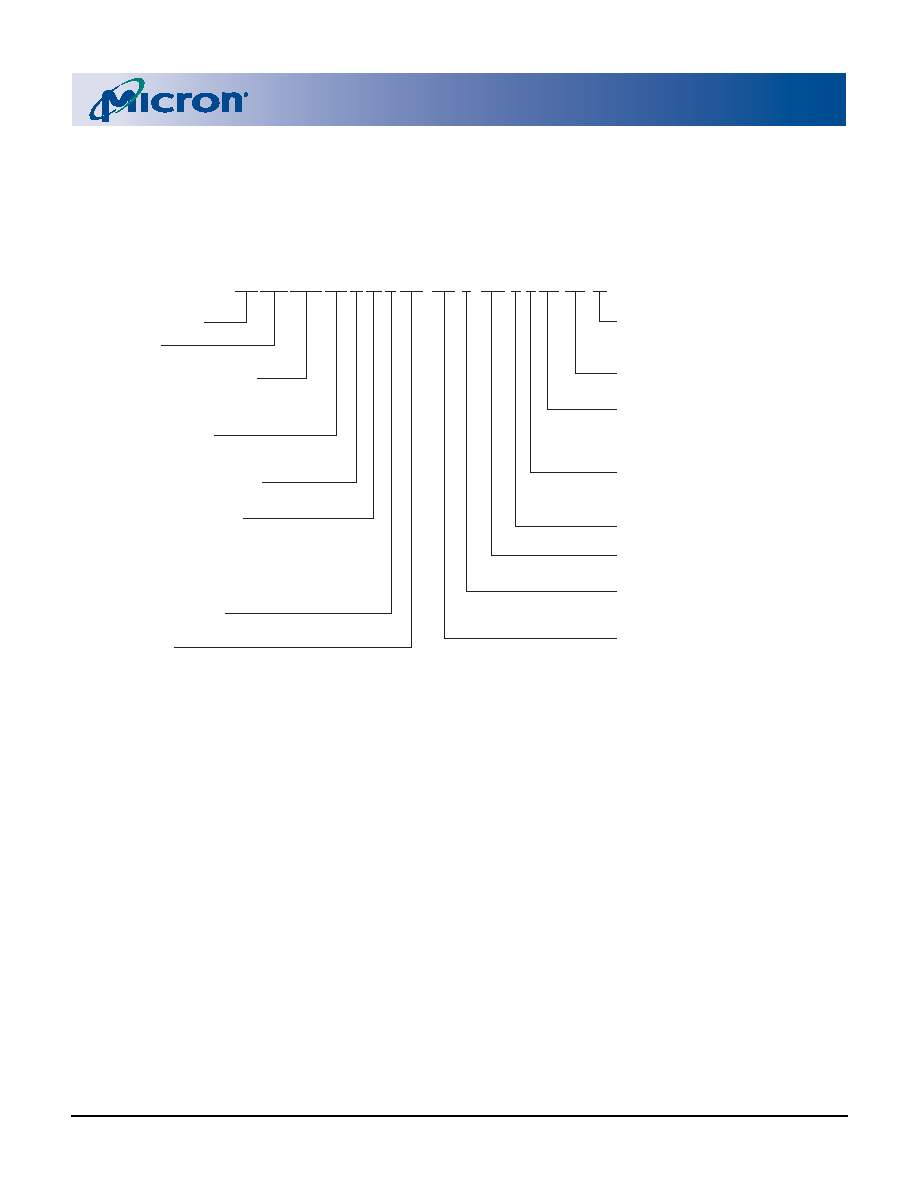
Part Number Information
Micron’s combination memory devices are available
with several different combinations of features (see
Figure 4).
Figure 4: Part Number Chart
NOTE:
1. The first character in this field refers to Flash die #2. The second character in this field refers to Flash die #1.
2. Contact factory for availability.
Valid Part Number Combinations
After building the part number from the part num-
ber chart above, please go to Micron’s Part Marking
Decoder Web site at www.micron.com/decoder to ver-
ify that the part number is offered and valid. If the
device required is not on this list, please contact the
factory.
Device Marking
Due to the size of the package, the Micron standard
part number is not printed on the top of each device.
Instead, an abbreviated device mark comprised of a
five-digit alphanumeric code is used. The abbreviated
device marks are cross-referenced to the Micron part
numbers at www.micron.com/decoder. To view the
location of the abbreviated mark on the device, please
refer to customer service note CSN-11, “Product Mark/
Label,” at www.micron.com/csn.
Micron Technology
Flash Family
28C = Dual-Supply Flash/CellularRAM Combo
Density/Organization/Banks
128 = two 64Mb (4,096K x 16)
bank x = 5 Multibank 32 Banks
(all banks have the same dimensions)
Flash Access Time
F60 = 60ns2
F70 = 70ns
CellularRAM Density
32 = 32Mb CellularRAM (2 Meg x 16)
64 = 64Mb CellularRAM (4 Meg x 16)
Flash Read Operation
W = Flash Async/Page/Burst
Package Code
FW = 77-ball FBGA (Standard) 8 x 10 grid
BW = 77-ball FBGA (Lead-free) 8 x 10 grid2
Operating Temperature Range
WT = Wireless (-25C to +85C)
Flash Burst Frequency
5 = 54 MHz
6 = 66 MHz2
Flash Boot Block Starting Address1
TT = Top boot/Top boot
TB = Top boot/Bottom boot
BT = Bottom boot/Top boot
BB = Bottom boot/Bottom boot
Operating Voltage Range
18
VCC
= 1.70V–1.95V
VCCQ = 1.70V–2.24V
30
VCC
= 1.70V–1.95V
VCCQ = 2.20V–3.30V
CE Select/Special Mark
E = Dual CE Flash with Burst CellularRAM Memory
Production Status
Blank = Production
ES = Engineering Samples
QS = Qualification Samples
MT28C 1285 64 W18 E FW -F70 5 -P85 6
BB WT ES
Flash Manufacturer's
Identification Code
None = Micron (2Ch)
K = Intel (89h)
CellularRAM Access Time
P70 = 70ns
P85 = 85ns
CellularRAM Burst Frequency
6 = 66 MHz
相關(guān)PDF資料 |
PDF描述 |
|---|---|
| MT28C128564W18EFW-F606P856KTBWT | SPECIALTY MEMORY CIRCUIT, PBGA77 |
| MT28C128564W18EFW-F606P856TBWT | SPECIALTY MEMORY CIRCUIT, PBGA77 |
| MT28C128564W18EFW-F705P706KBBWT | SPECIALTY MEMORY CIRCUIT, PBGA77 |
| MT28C256564W18SBT-F605P85BBWT | SPECIALTY MEMORY CIRCUIT, PBGA88 |
| MT28C256564W18SBT-F705P70BTWT | SPECIALTY MEMORY CIRCUIT, PBGA88 |
相關(guān)代理商/技術(shù)參數(shù) |
參數(shù)描述 |
|---|---|
| MT28C3212P2FL | 制造商:MICRON 制造商全稱:Micron Technology 功能描述:FLASH AND SRAM COMBO MEMORY |
| MT28C3212P2NFL | 制造商:MICRON 制造商全稱:Micron Technology 功能描述:FLASH AND SRAM COMBO MEMORY |
| MT28C3214P2FL | 制造商:MICRON 制造商全稱:Micron Technology 功能描述:FLASH AND SRAM COMBO MEMORY |
| MT28C3214P2FL-10 BET | 制造商:Micron Technology Inc 功能描述: |
| MT28C3214P2FL-10 BET TR | 制造商:Micron Technology Inc 功能描述: |
發(fā)布緊急采購,3分鐘左右您將得到回復(fù)。