- 您現(xiàn)在的位置:買賣IC網(wǎng) > PDF目錄383644 > MT8986 (Mitel Networks Corporation) Multiple Rate Digital Switch(多速率數(shù)字開關(guān)) PDF資料下載
參數(shù)資料
| 型號: | MT8986 |
| 廠商: | Mitel Networks Corporation |
| 英文描述: | Multiple Rate Digital Switch(多速率數(shù)字開關(guān)) |
| 中文描述: | 多速率數(shù)字交換機(jī)(多速率數(shù)字開關(guān)) |
| 文件頁數(shù): | 9/42頁 |
| 文件大小: | 249K |
| 代理商: | MT8986 |
第1頁第2頁第3頁第4頁第5頁第6頁第7頁第8頁當(dāng)前第9頁第10頁第11頁第12頁第13頁第14頁第15頁第16頁第17頁第18頁第19頁第20頁第21頁第22頁第23頁第24頁第25頁第26頁第27頁第28頁第29頁第30頁第31頁第32頁第33頁第34頁第35頁第36頁第37頁第38頁第39頁第40頁第41頁第42頁
MT8986
2-71
Register (FIO). If this function is not required in the
user's applications, the FIO register should be set up
during system initialization to a state where offset
functions are disabled.
Delay Through the MT8986
The switching of information from the input serial
streams to the output serial streams results in a
delay. Depending on the type of information to be
switched, the MT8986 device can be programmed to
perform time-slot interchange functions with different
throughput delay capabilities on a per-channel basis.
For voice applications, variable throughput delay can
be selected ensuring minimum delay between input
and output data. In wideband data applications,
constant
throughput
delay
maintaining the frame integrity of the information
through the switch.
can
be
selected
The delay through the MT8986 device varies
according to the type of throughput delay selected in
the V/C bit of the connect memory high.
Variable Throughput Delay Mode (V/C bit = 0)
Identical I/O Data Rates
The delay in this mode is dependent on the
combination of source and destination channels and
it is independent of the input and output streams.
The minimum delay achievable in the MT8986
depends on the data rate selected for the serial
streams. For instance, for 2.048 Mb/s the minimum
delay achieved corresponds to three time-slots. For
4.096 Mb/s it corresponds to five time-slots while for
8.192 Mb/s it is nine time-slots. Switching
configurations with input and output channels that
provides more than its corresponding minimum
throughput delay, will have a throughput delay equal
to the difference between the output and input
channels; i.e., the throughput delay will be less than
one frame period. Table 3a shows the MT8986
throughput delay for each data rate operation.
Different I/O Data Rates
Except for 2 Mb/s to 4 Mb/s and 2 Mb/s to 8 Mb/s
rate conversion operations, the throughput delay in
the MT8986 may vary according to the output stream
used for switching.
Table 3b explains the worst case conditions for the
throughput delay when different I/O data rate
switching configurations are used.
Constant Throughput Delay mode (V/C bit = 1)
In this mode frame sequence integrity is maintained
in both Identical and Different I/O Data Rate
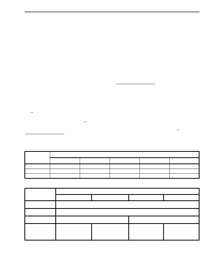
Table 3a. Variable Throughput Delay Values for Identical I/O Rate Applications
n= input channel, t.s. = time-slot
Table 3b. Min/Max Throughput Delay Values for Different I/O Rate Applications
Notes:
dmin and dmax are measured in time-slots and at the point in time when the output channel is completely shifted out.
t.s. = time-slot
fr. = 125
μ
s frame
2 Mb/s t.s. = 3.9
μ
s
4 Mb/s t.s. = 1.95
μ
s
8 Mb/s t.s. = 0.975
μ
s
Input Rate
Output Channel (# m)
m < n
m=n, n+1, n+2
m-n + 32 t.s.
m-n + 64 t.s.
m-n + 128 t.s.
m= n+3, n+4
m-n t.s.
m-n+64 t.s.
m-n+128 t.s.
m=n+5, .. n+8
m-n t.s.
m-n t.s.
m-n+128 t.s.
m > n+8
m-n t.s.
m-n t.s.
m-n t.s.
2.048 Mb/s
4.096 Mb/s
8.192 Mb/s
32-(n-m) t.s.
64-(n-m) t.s.
128-(n-m) t.s.
I/O Data Rate
Configuration
Output Stream Used
0, 1
2, 3
4, 5
6, 7
2 Mb/s to 4 Mb/s
dmin=5x 4Mb/s t.s.
dmax=1 fr.+(4x 4Mb/s t.s.)
dmin=9x 8Mb/s t.s.
dmax=1 fr.+(8x 8Mb/s t.s.)
dmin=3x 2Mb/s t.s.
dmax=1 fr.+(2x 2Mb/s t.s.)
dmin=3x 2Mb/s t.s.
dmax=1 fr.+(2x 2Mb/s
2 Mb/s to 8 Mb/s
4 Mb/s to 2 Mb/s
dmin=(2x 2Mb/s t.s.)+(1x 4Mb/s t.s.)
dmax=1 fr.+(1x 2Mb/s t.s.)+(1x 4Mb/s t.s.)
dmin=(2x 2Mb/s t.s.)+
(2x 8Mb/s t.s.)
dmax=1 fr.+(1x 2Mb/s
t.s.)+(2x 8Mb/s t.s.)
8 Mb/s to 2 Mb/s
t.s.)
dmin=(2x 2Mb/s t.s.)+
(3x 8Mb/s t.s.)
dmax=1 fr.+(1x 2Mb/s
t.s.)+(3x 8Mb/s t.s.)
dmin=(2x 2Mb/s t.s.)+
(1x 8Mb/s t.s.)
dmax=1 fr.+(1x 2Mb/s
t.s.)+(1x 8Mb/s t.s.)
相關(guān)PDF資料 |
PDF描述 |
|---|---|
| MT8992BC | Digital Telephone with HDLC |
| MT8993BC | Digital Telephone with HDLC |
| MT89L80 | Digital Switch(數(shù)字開關(guān)) |
| MT89L85 | Enhanced Digital Switch(加強(qiáng)型數(shù)字開關(guān)) |
| MT89L85 | CMOS ST-BUS⑩ FAMILY Enhanced Digital Switch |
相關(guān)代理商/技術(shù)參數(shù) |
參數(shù)描述 |
|---|---|
| MT8986AC | 制造商:MITEL 制造商全稱:Mitel Networks Corporation 功能描述:CMOS ST-BUS⑩ FAMILY Multiple Rate Digital Switch |
| MT8986AE | 制造商:Microsemi Corporation 功能描述: |
| MT8986AE1 | 制造商:Microsemi Corporation 功能描述:PB FREE MULTIPLE RATE DIGITAL SWITCH 制造商:Microsemi Corporation 功能描述:SWIT FABRIC 256 X 256/512 X 256/128 X 128 131.072MBPS 5V 40P - Rail/Tube 制造商:MICROSEMI CONSUMER MEDICAL PRODUCT GROUP 功能描述:IC TDM/TSI SWITCH 512X256 40PDIP 制造商:Microsemi Corporation 功能描述:IC TDM/TSI SWITCH 512X256 40PDIP |
| MT8986AL | 制造商:Microsemi Corporation 功能描述:SWIT FABRIC 256 X 256/512 X 256/128 X 128 131.072MBPS 5V 44M - Trays 制造商:Zarlink Semiconductor Inc 功能描述:SWIT FABRIC 256 X 256/512 X 256/128 X 128 131.072MBPS 5V 44M - Trays |
| MT8986AL1 | 制造商:Microsemi Corporation 功能描述:SWIT FABRIC 256 X 256/512 X 256/128 X 128 131.072MBPS 5V 44M - Trays 制造商:Zarlink Semiconductor Inc 功能描述:SWIT FABRIC 256 X 256/512 X 256/128 X 128 131.072MBPS 5V 44M - Trays |
發(fā)布緊急采購,3分鐘左右您將得到回復(fù)。