- 您現(xiàn)在的位置:買(mǎi)賣(mài)IC網(wǎng) > PDF目錄68019 > MTA85811-04I/SS 8-BIT, OTPROM, 4 MHz, RISC MICROCONTROLLER, PDSO20 PDF資料下載
參數(shù)資料
| 型號(hào): | MTA85811-04I/SS |
| 元件分類: | 微控制器/微處理器 |
| 英文描述: | 8-BIT, OTPROM, 4 MHz, RISC MICROCONTROLLER, PDSO20 |
| 封裝: | 0.209 INCH, PLASTIC, SSOP-20 |
| 文件頁(yè)數(shù): | 48/72頁(yè) |
| 文件大小: | 760K |
| 代理商: | MTA85811-04I/SS |
第1頁(yè)第2頁(yè)第3頁(yè)第4頁(yè)第5頁(yè)第6頁(yè)第7頁(yè)第8頁(yè)第9頁(yè)第10頁(yè)第11頁(yè)第12頁(yè)第13頁(yè)第14頁(yè)第15頁(yè)第16頁(yè)第17頁(yè)第18頁(yè)第19頁(yè)第20頁(yè)第21頁(yè)第22頁(yè)第23頁(yè)第24頁(yè)第25頁(yè)第26頁(yè)第27頁(yè)第28頁(yè)第29頁(yè)第30頁(yè)第31頁(yè)第32頁(yè)第33頁(yè)第34頁(yè)第35頁(yè)第36頁(yè)第37頁(yè)第38頁(yè)第39頁(yè)第40頁(yè)第41頁(yè)第42頁(yè)第43頁(yè)第44頁(yè)第45頁(yè)第46頁(yè)第47頁(yè)當(dāng)前第48頁(yè)第49頁(yè)第50頁(yè)第51頁(yè)第52頁(yè)第53頁(yè)第54頁(yè)第55頁(yè)第56頁(yè)第57頁(yè)第58頁(yè)第59頁(yè)第60頁(yè)第61頁(yè)第62頁(yè)第63頁(yè)第64頁(yè)第65頁(yè)第66頁(yè)第67頁(yè)第68頁(yè)第69頁(yè)第70頁(yè)第71頁(yè)第72頁(yè)
MTA85XXX
DS40115C-page 52
1995 Microchip Technology Inc.
17.0
EEPROM BUS DESCRIPTION
The MTA85XXX supports a bidirectional two wire bus
and data transmission protocol. A device that sends
data onto the bus is defined as transmitter, and a
device receiving data as receiver. The bus has to be
controlled by a master device (microcontroller) which
generates the
serial clock (SCL), controls the bus
access,
and
generates
the
START
and
STOP
conditions, while the EEPROM (24LC01B/02B) works
as slave. Both master and slave can operate as
transmitter
or
receiver
but
the
master
device
determines which mode is activated.
17.1
Bus Characteristics
The following bus protocol has been defined:
- Data transfer may be initiated only when the
bus is not busy.
- During data transfer, the data line must
remain stable whenever the clock line is
HIGH. Changes in the data line while the
clock line is HIGH will be interpreted as a
START or STOP condition.
Accordingly, the following bus conditions have been
defined (Figure 17-1):
17.1.1
BUS NOT BUSY (A)
Both data and clock lines remain HIGH.
17.1.2
START DATA TRANSFER (B)
A HIGH to LOW transition of the SDA line while the
clock (SCL) is HIGH determines a START condition. All
commands must be preceded by a START condition.
17.1.3
STOP DATA TRANSFER (C)
A LOW to HIGH transition of the SDA line while the
clock (SCL) is HIGH determines a STOP condition. All
operations must be ended with a STOP condition.
17.1.4
DATA VALID (D)
The state of the data line represents valid data when,
after a START condition, the data line is stable for the
duration of the HIGH period of the clock signal.
The data on the line must be changed during the LOW
period of the clock signal. There is one clock pulse per
bit of data.
Each data transfer is initiated with a START condition
and terminated with a STOP condition. The number of
the data bytes transferred between the START and
STOP conditions is determined by the master device
and is theoretically unlimited, although only the last
sixteen will be stored when doing a write operation.
When an overwrite does occur it will replace data in a
first in first out fashion.
17.1.5
ACKNOWLEDGE
Each receiving device, when addressed, is obliged to
generate an acknowledge after the reception of each
byte. The master device must generate an extra clock
pulse which is associated with this acknowledge bit.
The device that acknowledges has to pull down the
SDA line during the acknowledge clock pulse in such a
way that the SDA line is stable LOW during the HIGH
period of the acknowledge related clock pulse. Of
course, setup and hold times must be taken into
account. A master must signal an end of data to the
slave by not generating an acknowledge bit on the last
byte that has been clocked out of the slave. In this
case, the slave must leave the data line HIGH to enable
the master to generate the STOP condition.
* Note: The EEPROM does not generate any
acknowledge bits if an internal pro-
gramming cycle is in progress.
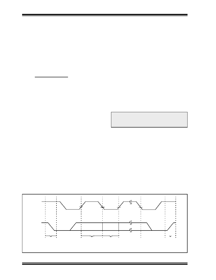
FIGURE 17-1: DATA TRANSFER SEQUENCE ON THE SERIAL BUS
AAAA
AA
SCL
SDA
(A)
(B)
START
(C)
(A)
(D)
Address
or
Acknowledge
Valid
Data Allowed
to Change
STOP
Condition
相關(guān)PDF資料 |
PDF描述 |
|---|---|
| MTA85802-10I/SS | 8-BIT, OTPROM, 10 MHz, RISC MICROCONTROLLER, PDSO20 |
| MTA85801-10I/SS | 8-BIT, OTPROM, 10 MHz, RISC MICROCONTROLLER, PDSO20 |
| MTA85812-10I/SS | 8-BIT, OTPROM, 10 MHz, RISC MICROCONTROLLER, PDSO20 |
| MTA85402S-04I/SS | 8-BIT, OTPROM, 4 MHz, RISC MICROCONTROLLER, PDSO20 |
| MTA85801-04I/SS | 8-BIT, OTPROM, 4 MHz, RISC MICROCONTROLLER, PDSO20 |
相關(guān)代理商/技術(shù)參數(shù) |
參數(shù)描述 |
|---|---|
| MTA8808 | 制造商:Pulse Electronics Corporation 功能描述: |
| MTA8ATF1G64AZ-2G3B1 | 功能描述:Memory Module DDR4 SDRAM 8GB 2400MT/s 288-UDIMM 制造商:micron technology inc. 系列:- 零件狀態(tài):在售 存儲(chǔ)器類型:DDR4 SDRAM 存儲(chǔ)容量:8GB 速度:2400MT/s 封裝/外殼:288-UDIMM 標(biāo)準(zhǔn)包裝:1 |
| MTA8ATF1G64HZ-2G3B1 | 功能描述:Memory Module DDR4 SDRAM 8GB 2400MT/s 260-SODIMM 制造商:micron technology inc. 系列:- 零件狀態(tài):在售 存儲(chǔ)器類型:DDR4 SDRAM 存儲(chǔ)容量:8GB 速度:2400MT/s 封裝/外殼:260-SODIMM 標(biāo)準(zhǔn)包裝:1 |
| MTA8D50 | 制造商:Mallory Sonalert Products Inc 功能描述:Molded Tubular Aluminum Electrolytic Axial Leads Capacitor - 8uF 50dcV -10+100% |
| MTA90A | 制造商:LIUJING 制造商全稱:LIUJING 功能描述:可控硅(晶閘管) |
發(fā)布緊急采購(gòu),3分鐘左右您將得到回復(fù)。