- 您現(xiàn)在的位置:買賣IC網(wǎng) > PDF目錄359242 > MV8870-1 (Zarlink Semiconductor Inc.) INTERGRATED DTMF RECEIVER PDF資料下載
參數(shù)資料
| 型號(hào): | MV8870-1 |
| 廠商: | Zarlink Semiconductor Inc. |
| 英文描述: | INTERGRATED DTMF RECEIVER |
| 中文描述: | 集成雙音多頻接收器 |
| 文件頁(yè)數(shù): | 6/12頁(yè) |
| 文件大小: | 205K |
| 代理商: | MV8870-1 |

MV8870/MV8870-1
5
DIFFERENTIAL INPUT CONFIGURATION
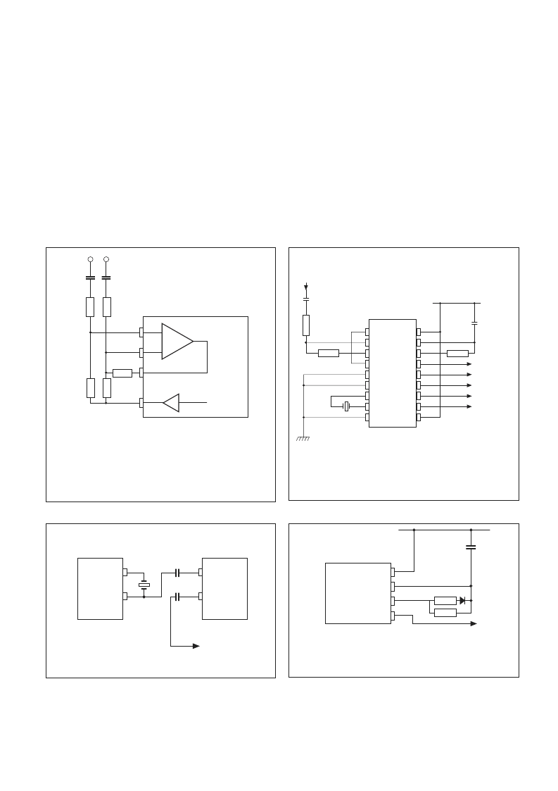
The input arrangement of the MV8870 / MV8870-1
provides a differential input op. amp. and a bias source (V
REF
)
to bias the inputs at mid-rail. The gain may be adjusted through
a feedback resistor from the op. amp. output (GS). In a single-
ended configuration the input pins are connected as shown in
Fig. 7 where the op. amp. is connected to give unity gain and
the V
REF
pin biases the input at (V
DD
÷
2).
Fig.9 shows the differential configuration. In this circuit gain
is adjusted through the feedback resistor R5.
CRYSTAL OSCILLATOR
The internal clock circuit is completed with the addition of
an external 3.58MHz crystal which is normally connected as
shown in Fig. 7. However it is possible to configure several
MV8870 / MV8870-1 devices to use only a single oscillator
crystal.
The devices are chained together with the oscillator output
of the first device in the chain capacitively coupled to the
oscillator input of the second device and so on down the chain.
The details are shown in Fig. 10. Precision balancing
capacitors are not required as problems of unbalanced loading
are not a concern.
RECEIVER SYSTEM FOR BT SPECIFICATION POR 1151
The circuit shown in Fig.11 illustrates the use of the
MV8870-1 in a typical receiver system. The BT specification
defines the non-operate level as input signals below 34 dBm.
This is obtained by choosing R1 and R2 to give 3dB of
attenuation so that an input of 34 dBm corresponds to -37 dBm
at the op. amp. output pin (GS). The tolerances on R3 and C2
give a tolerance on guard time of 6%. For better performance
the non-symmetric guard time circuit shown in Fig.12 is
recommended.
C2
C1
R4
R1
R3
R2
R5
IN+
IN-
GS
V
REF
1
2
3
4
+
-
MV8870/
MV8870-1
Differential Input Amplifier
C1 = C2 = 0.01
μ
F
R1 = R4 = R5 = 100k
R2 = 60k
R3 = R2R5
÷
(R2 + R5)
Voltage Gain
(A
V
diff) = R5
÷
R1
Input Impedance
Z
INDIFF
= 2[R1
2
+ (1
÷
wC)
2
]
1
/
2
Resistors are
±
1%
Capacitors are
±
5%
IN+
IN-
GS
V
REF
SEL
PD
OSC1
OSC2
V
SS
1
2
3
4
5
6
7
8
9
18
17
16
15
14
13
12
11
10
V
DD
St/GT
ESt
StD
Q4
Q3
Q2
Q1
TOE
R3
C2
V
DD
R2
R1
C1
X
DTMF
R1 = 102k
±
1%
R2 = 71.5k
±
1%
R3 = 390k
±
1%
C1, C2 = 0.1
μ
F
±
5%
X = 3.579545MHz
±
0.1%
DECODED
OUTPUT
}
MV8870/
MV8870-1
MV8870/
MV8870-1
MV8870/
MV8870-1
OSC1
OSC2
7
8
7
8
C
C
OSC1
OSC2
X
To OSC1
of next
MV8870/
MV8870-1
C = 30pF
X = 3.57945MHz
18
17
16
15
R1
R2
C
V
DD
V
DD
St/GT
ESt
StD
MV8870/
MV8870-1
t
GTA
= R1C In {V
DD
÷
V
TSt
}
t
GTP
= R
P
C In {V
DD
÷
[V
DD
- V
TSt
]}
R
P
= R1R2
÷
{R1 + R2}
R1 = 368k
±
1%
R2 = 2.2m
±
1%
C = 0.1
μ
F
±
5%
Figure 9: Differential input configuration
Figure 11: Single ended circuit for BT/CEPT Specs
Figure 10: Oscillator circuit
Figure 12: Non-symmetric guard time circuit
相關(guān)PDF資料 |
PDF描述 |
|---|---|
| MV95308 | 30MHz 8-BIT CMOS VIDEO DAC |
| MV95308ADG | 30MHz 8-BIT CMOS VIDEO DAC |
| MV95308CDP | 30MHz 8-BIT CMOS VIDEO DAC |
| MV95308CMP | 30MHz 8-BIT CMOS VIDEO DAC |
| MVM302P12 | Analog Miscellaneous |
相關(guān)代理商/技術(shù)參數(shù) |
參數(shù)描述 |
|---|---|
| MV8870-1/DP | 制造商:未知廠家 制造商全稱:未知廠家 功能描述:DTMF Receiver |
| MV8870-1DP | 制造商:未知廠家 制造商全稱:未知廠家 功能描述:Telecommunication IC |
| MV8870-1MP | 制造商:未知廠家 制造商全稱:未知廠家 功能描述:DTMF Receiver |
| MV8870DG | 制造商:未知廠家 制造商全稱:未知廠家 功能描述:DTMF Receiver |
| MV8870HP | 制造商:未知廠家 制造商全稱:未知廠家 功能描述:DTMF Receiver |
發(fā)布緊急采購(gòu),3分鐘左右您將得到回復(fù)。