- 您現(xiàn)在的位置:買賣IC網(wǎng) > PDF目錄361076 > NBC12429 (ON SEMICONDUCTOR) 3.3V/5V Programmable PLL Synthesized Clock Generator(3.3V/5V可編程PLL合成時(shí)鐘發(fā)生器) PDF資料下載
參數(shù)資料
| 型號(hào): | NBC12429 |
| 廠商: | ON SEMICONDUCTOR |
| 英文描述: | 3.3V/5V Programmable PLL Synthesized Clock Generator(3.3V/5V可編程PLL合成時(shí)鐘發(fā)生器) |
| 中文描述: | 3.3V/5V的可編程鎖相環(huán)路合成時(shí)鐘發(fā)生器(3.3V/5V的可編程PLL頻率合成時(shí)鐘發(fā)生器) |
| 文件頁數(shù): | 4/20頁 |
| 文件大?。?/td> | 351K |
| 代理商: | NBC12429 |
NBC12429, NBC12429A
http://onsemi.com
4
ThefollowinggivesabriefdescriptionofthefunctionalityoftheNBC12429andNBC12429AInputsandOutputs.Unless
explicitlystated,allinputsareCMOS/TTLcompatiblewitheitherpulluporpulldownresistors.ThePECLoutputsarecapable
of driving two series terminated 50
Ω
transmission lines on the incident edge.
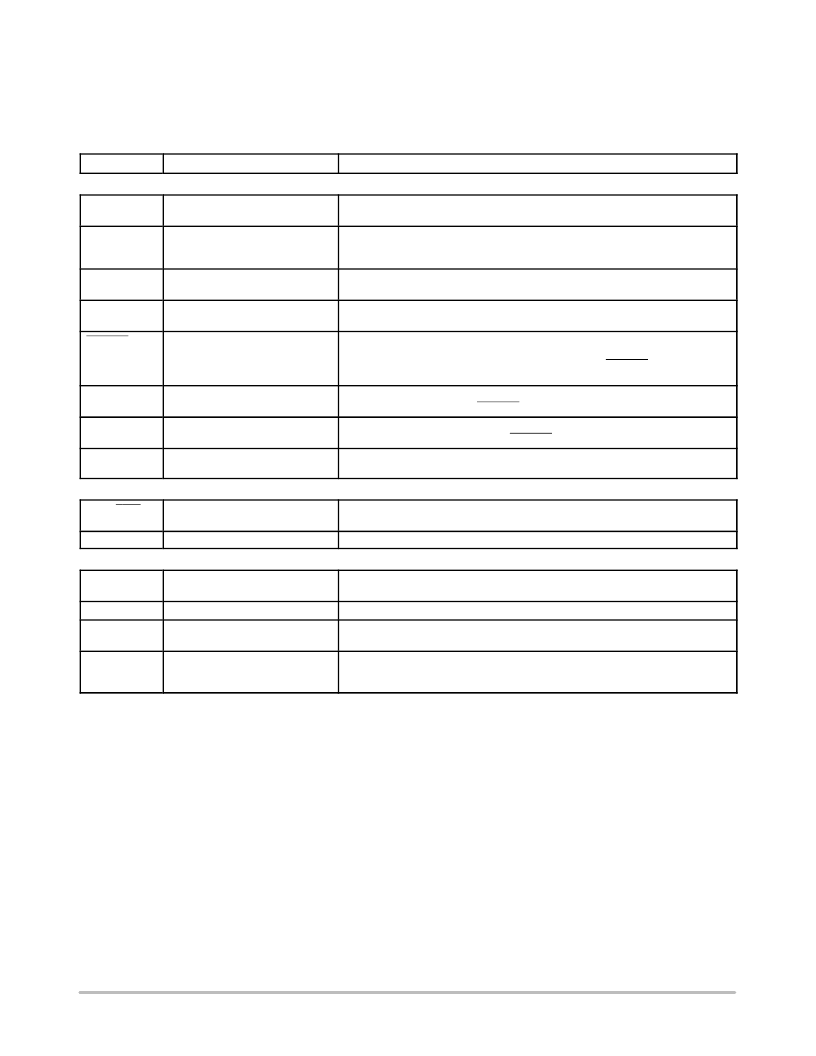
Table 3. PIN FUNCTION DESCRIPTION
Pin Name
Function
Description
INPUTS
XTAL1, XTAL2
Crystal Inputs
These pins form an oscillator when connected to an external series--resonant
crystal.
S_LOAD*
CMOS/TTL Serial Latch Input
(Internal Pulldown Resistor)
This pin loads the configuration latches with the contents of the shift registers. The
latches will be transparent when this signal is HIGH; thus, the data must be stable
on the HIGH--to--LOW transition of S_LOAD for proper operation.
S_DATA*
CMOS/TTL Serial Data Input
(Internal Pulldown Resistor)
This pin acts as the data input to the serial configuration shift registers.
S_CLOCK*
CMOS/TTL Serial Clock Input
(Internal Pulldown Resistor)
This pin serves to clock the serial configuration shift registers. Data from S_DATA
is sampled on the rising edge.
P_LOAD**
CMOS/TTL Parallel Latch Input
(Internal Pullup Resistor)
This pin loads the configuration latches with the contents of the parallel inputs.
The latches will be transparent when this signal is LOW; therefore, the parallel
data must be stable on the LOW--to--HIGH transition of P_LOAD for proper opera-
tion.
M[8:0]**
CMOS/TTL PLL Loop Divider
Inputs (Internal Pullup Resistor)
These pins are used to configure the PLL loop divider. They are sampled on the
LOW--to--HIGH transition of P_LOAD. M[8] is the MSB, M[0] is the LSB.
N[1:0]**
CMOS/TTL Output Divider Inputs
(Internal Pullup Resistor)
These pins are used to configure the output divider modulus. They are sampled
on the LOW--to--HIGH transition of P_LOAD.
OE**
CMOS/TTL Output Enable Input
(Internal Pullup Resistor)
Active HIGH Output Enable. The Enable is synchronous to eliminate possibility of
runt pulse generation on the FOUT output.
OUTPUTS
F
OUT
, F
OUT
PECL Differential Outputs
These differential, positive--referenced ECL signals (PECL) are the outputs of the
synthesizer.
TEST
CMOS/TTL Output
The function of this output is determined by the serial configuration bits T[2:0].
POWER
V
CC
Positive Supply for the Logic
The positive supply for the internal logic and output buffer of the chip, and is con-
nected to +3.3 V or +5.0 V.
PLL_V
CC
GND
Positive Supply for the PLL
This is the positive supply for the PLL and is connected to +3.3 V or +5.0 V.
Negative Power Supply
These pins are the negative supply for the chip and are normally all connected to
ground.
--
Exposed Pad for QFN--32 only
The Exposed Pad (EP) on the QFN--32 package bottom is thermally connected to
the die for improved heat transfer out of package. The exposed pad must be at-
tached to a heat--sinking conduit. The pad is electrically connected to GND.
*
** When left Open, these inputs will default HIGH.
When left Open, these inputs will default LOW.
相關(guān)PDF資料 |
PDF描述 |
|---|---|
| NBC12429A | 3.3V/5V Programmable PLL Synthesized Clock Generator(3.3V/5V可編程PLL合成時(shí)鐘發(fā)生器) |
| NBC12430 | 3.3V/5V Programmable PLL Synthesized Clock Generator(3.3V/5V可編程PLL合成時(shí)鐘發(fā)生器) |
| NBC12430A | 3.3V/5V Programmable PLL Synthesized Clock Generator(3.3V/5V可編程PLL合成時(shí)鐘發(fā)生器) |
| NBC12439A | 3.3V/5V Programmable PLL Synthesized Clock Generator(3.3V/5V可編程PLL合成時(shí)鐘發(fā)生器) |
| NBC12439 | 3.3V/5V Programmable PLL Synthesized Clock Generator(3.3V/5V可編程PLL合成時(shí)鐘發(fā)生器) |
相關(guān)代理商/技術(shù)參數(shù) |
參數(shù)描述 |
|---|---|
| NBC12429/D | 制造商:ONSEMI 制造商全稱:ON Semiconductor 功能描述:3.3 V/5 V Programmable PLL Synthesized Clock Generator (25 to 400 MHz) |
| NBC12429_07 | 制造商:ONSEMI 制造商全稱:ON Semiconductor 功能描述:3.3V/5V Programmable PLL Synthesized Clock Generator |
| NBC12429A | 制造商:ONSEMI 制造商全稱:ON Semiconductor 功能描述:3.3V/5V Programmable PLL Synthesized Clock Generator |
| NBC12429AFA | 功能描述:鎖相環(huán) - PLL 3.3V/5V Programmable RoHS:否 制造商:Silicon Labs 類型:PLL Clock Multiplier 電路數(shù)量:1 最大輸入頻率:710 MHz 最小輸入頻率:0.002 MHz 輸出頻率范圍:0.002 MHz to 808 MHz 電源電壓-最大:3.63 V 電源電壓-最小:1.71 V 最大工作溫度:+ 85 C 最小工作溫度:- 40 C 封裝 / 箱體:QFN-36 封裝:Tray |
| NBC12429AFAG | 功能描述:鎖相環(huán) - PLL 3.3V/5V Programmable PLL Clock Generator RoHS:否 制造商:Silicon Labs 類型:PLL Clock Multiplier 電路數(shù)量:1 最大輸入頻率:710 MHz 最小輸入頻率:0.002 MHz 輸出頻率范圍:0.002 MHz to 808 MHz 電源電壓-最大:3.63 V 電源電壓-最小:1.71 V 最大工作溫度:+ 85 C 最小工作溫度:- 40 C 封裝 / 箱體:QFN-36 封裝:Tray |
發(fā)布緊急采購,3分鐘左右您將得到回復(fù)。