- 您現(xiàn)在的位置:買(mǎi)賣(mài)IC網(wǎng) > PDF目錄299575 > OR3T806PS240-DB (LATTICE SEMICONDUCTOR CORP) FPGA, 484 CLBS, 116000 GATES, PQFP240 PDF資料下載
參數(shù)資料
| 型號(hào): | OR3T806PS240-DB |
| 廠商: | LATTICE SEMICONDUCTOR CORP |
| 元件分類(lèi): | FPGA |
| 英文描述: | FPGA, 484 CLBS, 116000 GATES, PQFP240 |
| 封裝: | PLASTIC, SQFP2-240 |
| 文件頁(yè)數(shù): | 163/203頁(yè) |
| 文件大?。?/td> | 1368K |
| 代理商: | OR3T806PS240-DB |
第1頁(yè)第2頁(yè)第3頁(yè)第4頁(yè)第5頁(yè)第6頁(yè)第7頁(yè)第8頁(yè)第9頁(yè)第10頁(yè)第11頁(yè)第12頁(yè)第13頁(yè)第14頁(yè)第15頁(yè)第16頁(yè)第17頁(yè)第18頁(yè)第19頁(yè)第20頁(yè)第21頁(yè)第22頁(yè)第23頁(yè)第24頁(yè)第25頁(yè)第26頁(yè)第27頁(yè)第28頁(yè)第29頁(yè)第30頁(yè)第31頁(yè)第32頁(yè)第33頁(yè)第34頁(yè)第35頁(yè)第36頁(yè)第37頁(yè)第38頁(yè)第39頁(yè)第40頁(yè)第41頁(yè)第42頁(yè)第43頁(yè)第44頁(yè)第45頁(yè)第46頁(yè)第47頁(yè)第48頁(yè)第49頁(yè)第50頁(yè)第51頁(yè)第52頁(yè)第53頁(yè)第54頁(yè)第55頁(yè)第56頁(yè)第57頁(yè)第58頁(yè)第59頁(yè)第60頁(yè)第61頁(yè)第62頁(yè)第63頁(yè)第64頁(yè)第65頁(yè)第66頁(yè)第67頁(yè)第68頁(yè)第69頁(yè)第70頁(yè)第71頁(yè)第72頁(yè)第73頁(yè)第74頁(yè)第75頁(yè)第76頁(yè)第77頁(yè)第78頁(yè)第79頁(yè)第80頁(yè)第81頁(yè)第82頁(yè)第83頁(yè)第84頁(yè)第85頁(yè)第86頁(yè)第87頁(yè)第88頁(yè)第89頁(yè)第90頁(yè)第91頁(yè)第92頁(yè)第93頁(yè)第94頁(yè)第95頁(yè)第96頁(yè)第97頁(yè)第98頁(yè)第99頁(yè)第100頁(yè)第101頁(yè)第102頁(yè)第103頁(yè)第104頁(yè)第105頁(yè)第106頁(yè)第107頁(yè)第108頁(yè)第109頁(yè)第110頁(yè)第111頁(yè)第112頁(yè)第113頁(yè)第114頁(yè)第115頁(yè)第116頁(yè)第117頁(yè)第118頁(yè)第119頁(yè)第120頁(yè)第121頁(yè)第122頁(yè)第123頁(yè)第124頁(yè)第125頁(yè)第126頁(yè)第127頁(yè)第128頁(yè)第129頁(yè)第130頁(yè)第131頁(yè)第132頁(yè)第133頁(yè)第134頁(yè)第135頁(yè)第136頁(yè)第137頁(yè)第138頁(yè)第139頁(yè)第140頁(yè)第141頁(yè)第142頁(yè)第143頁(yè)第144頁(yè)第145頁(yè)第146頁(yè)第147頁(yè)第148頁(yè)第149頁(yè)第150頁(yè)第151頁(yè)第152頁(yè)第153頁(yè)第154頁(yè)第155頁(yè)第156頁(yè)第157頁(yè)第158頁(yè)第159頁(yè)第160頁(yè)第161頁(yè)第162頁(yè)當(dāng)前第163頁(yè)第164頁(yè)第165頁(yè)第166頁(yè)第167頁(yè)第168頁(yè)第169頁(yè)第170頁(yè)第171頁(yè)第172頁(yè)第173頁(yè)第174頁(yè)第175頁(yè)第176頁(yè)第177頁(yè)第178頁(yè)第179頁(yè)第180頁(yè)第181頁(yè)第182頁(yè)第183頁(yè)第184頁(yè)第185頁(yè)第186頁(yè)第187頁(yè)第188頁(yè)第189頁(yè)第190頁(yè)第191頁(yè)第192頁(yè)第193頁(yè)第194頁(yè)第195頁(yè)第196頁(yè)第197頁(yè)第198頁(yè)第199頁(yè)第200頁(yè)第201頁(yè)第202頁(yè)第203頁(yè)
62
Lattice Semiconductor
Data Sheet
November 2006
ORCA Series 3C and 3T FPGAs
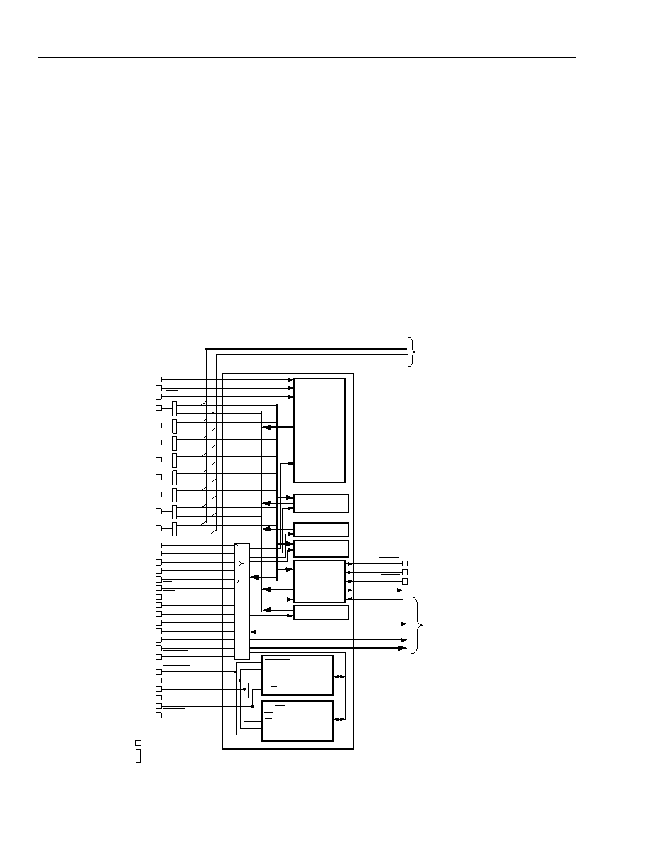
Microprocessor Interface (MPI)
The Series 3 FPGAs have a dedicated synchronous
microprocessor interface function block (see
Figure 42). The MPI is programmable to operate with
PowerPC MPC800 series microprocessors and Intel*
respectively, for compatible processors. The MPI imple-
ments an 8-bit interface to the host processor (
Pow-
erPC or i960) that can be used for conguration and
readback of the FPGA as well as for user-dened data
processing and general monitoring of FPGA function.
In addition to dedicated-function registers, the micro-
processor interface allows for the control of up to 16
user registers (RAM or ip-ops) in the FPGA logic. A
synchronous/asynchronous handshake procedure is
used to control transactions with user logic in the FPGA
array. There is also capability for the FPGA logic to
interrupt the host processor either by a hard interrupt or
by having the host processor poll the microprocessor
interface.
The control portion of the microprocessor interface is
available following powerup of the FPGA if the mode
pins specify MPI mode, even if the FPGA is not yet con-
gured. The mode pin (M[2:0]) settings can be found in
the FPGA Conguration Modes section of this data
sheet, and the setup and use of the MPI for congura-
tion is discussed in the MPI Setup and Control subsec-
tion. For postconguration use, the MPI must be
included in the conguration bit stream by using an MPI
library element in your design from the
ORCA macro
library, or by setting the MP_USER bit of the MPI con-
guration control register prior to the start of congura-
tion (MPI registers are discussed later).
*
Intel and i960 are registered trademarks of Intel Corporation.
5-5806(F)
Figure 42. MPI Block Diagram
DONE
RD_DATA
INIT
D7
D7IN
D7OUT
D6
D6IN
D6OUT
D5
D5IN
D5OUT
D4
D4IN
D4OUT
D3
D3IN
D3OUT
D2
D2IN
D2OUT
D1
D1IN
D1OUT
D0
D0IN
D0OUT
ORCAORCA 3C/Txxx MPI
STATUS
REGISTER
SCRATCHPAD
REGISTER
READBACK
DATA REGISTER
READBACK
ADDR REGISTER
CONTROL
REGISTERS
PART ID
REGISTERS
RESET
RD_CFG
PRGM
GSR
IRQ
TO GSR BLOCK
TO FPGA
ROUTING
USER_START
USER_END
WR_CTRL
A[3:0]
RDYRCV
CLK
ADS
ALE
W/R
i960 LOGIC
RD/WR
BT
TS
CLKOUT
TA
POWERPC LOGIC
DECODE/CONTROL
POWERPC
ONLY
A4
A3
A2
A1
A0
RD
CS0
CS1
CCLK
M3
M2
M1
M0
MPI_IRQ
MPI_ACK
MPI_CLK
MPI_STRB
MPI_ALE
MPI_RW
MPI_B1
TO FPGA
ROUTING
D[7:0]IN
D[7:0]OUT
DEVICE PAD
I/O BUFFER
Select
devices
have
been
discontinued.
See
Ordering
Information
section
for
product
status.
相關(guān)PDF資料 |
PDF描述 |
|---|---|
| OR3T807PS240-DB | FPGA, 484 CLBS, 116000 GATES, PQFP240 |
| OR3T55-4BA256I | FPGA, 324 CLBS, 40000 GATES, 80 MHz, PBGA256 |
| OR3T55-4BA256 | FPGA, 324 CLBS, 40000 GATES, 80 MHz, PBGA256 |
| OR3T55-4BA352I | FPGA, 324 CLBS, 40000 GATES, 80 MHz, PBGA352 |
| OR3T55-4BA352 | FPGA, 324 CLBS, 40000 GATES, 80 MHz, PBGA352 |
相關(guān)代理商/技術(shù)參數(shù) |
參數(shù)描述 |
|---|---|
| OR3T80-6PS240I | 制造商:AGERE 制造商全稱(chēng):AGERE 功能描述:3C and 3T Field-Programmable Gate Arrays |
| OR3T806PS240I-DB | 功能描述:FPGA - 現(xiàn)場(chǎng)可編程門(mén)陣列 3872 LUT 342 I/O RoHS:否 制造商:Altera Corporation 系列:Cyclone V E 柵極數(shù)量: 邏輯塊數(shù)量:943 內(nèi)嵌式塊RAM - EBR:1956 kbit 輸入/輸出端數(shù)量:128 最大工作頻率:800 MHz 工作電源電壓:1.1 V 最大工作溫度:+ 70 C 安裝風(fēng)格:SMD/SMT 封裝 / 箱體:FBGA-256 |
| OR3T806S208-DB | 功能描述:FPGA - 現(xiàn)場(chǎng)可編程門(mén)陣列 Use LatticeEC RoHS:否 制造商:Altera Corporation 系列:Cyclone V E 柵極數(shù)量: 邏輯塊數(shù)量:943 內(nèi)嵌式塊RAM - EBR:1956 kbit 輸入/輸出端數(shù)量:128 最大工作頻率:800 MHz 工作電源電壓:1.1 V 最大工作溫度:+ 70 C 安裝風(fēng)格:SMD/SMT 封裝 / 箱體:FBGA-256 |
| OR3T806S208I-DB | 功能描述:FPGA - 現(xiàn)場(chǎng)可編程門(mén)陣列 Use LatticeEC RoHS:否 制造商:Altera Corporation 系列:Cyclone V E 柵極數(shù)量: 邏輯塊數(shù)量:943 內(nèi)嵌式塊RAM - EBR:1956 kbit 輸入/輸出端數(shù)量:128 最大工作頻率:800 MHz 工作電源電壓:1.1 V 最大工作溫度:+ 70 C 安裝風(fēng)格:SMD/SMT 封裝 / 箱體:FBGA-256 |
| OR3T80-7BA352 | 制造商:Lattice Semiconductor Corporation 功能描述:Field-Programmable Gate Array, 484 Cell, 352 Pin, Plastic, BGA |
發(fā)布緊急采購(gòu),3分鐘左右您將得到回復(fù)。