- 您現(xiàn)在的位置:買賣IC網(wǎng) > PDF目錄378039 > PAL22V10Z-30I (Texas Instruments, Inc.) EPICE CMOS PROGRAMMABLE ARRAY LOGIC CIRCUITS PDF資料下載
參數(shù)資料
| 型號(hào): | PAL22V10Z-30I |
| 廠商: | Texas Instruments, Inc. |
| 英文描述: | EPICE CMOS PROGRAMMABLE ARRAY LOGIC CIRCUITS |
| 中文描述: | EPICE CMOS可編程陣列邏輯電路 |
| 文件頁(yè)數(shù): | 13/22頁(yè) |
| 文件大小: | 202K |
| 代理商: | PAL22V10Z-30I |
第1頁(yè)第2頁(yè)第3頁(yè)第4頁(yè)第5頁(yè)第6頁(yè)第7頁(yè)第8頁(yè)第9頁(yè)第10頁(yè)第11頁(yè)第12頁(yè)當(dāng)前第13頁(yè)第14頁(yè)第15頁(yè)第16頁(yè)第17頁(yè)第18頁(yè)第19頁(yè)第20頁(yè)第21頁(yè)第22頁(yè)
TICPAL22V10Z-25C, TICPAL22V10Z-30I
EPIC
CMOS PROGRAMMABLE ARRAY LOGIC CIRCUITS
SRPS007C – D3323, SEPTEMBER 1989 – REVISED FEBRUARY 1992
POST OFFICE BOX 655303
DALLAS, TEXAS 75265
13
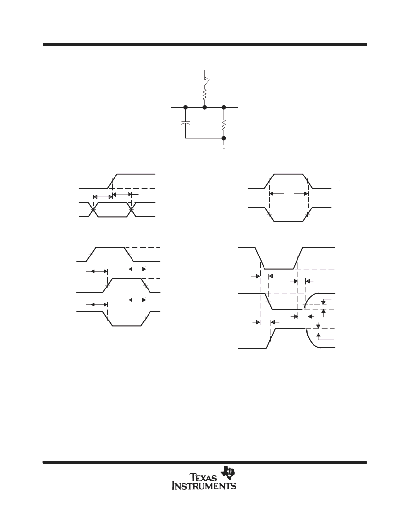
PARAMETER MEASUREMENT INFORMATION
tsu
S1
From Output
Under Test
Test
Point
CL
(see Note A)
LOAD CIRCUIT FOR
3-STATE OUTPUTS
3 V
0
1.5 V
1.5 V
th
1.5 V
CLK
Data
Input
Input
In-Phase
Output
Out-of-Phase
Output
(see Note D)
tpd
tpd
tpd
tpd
VOLTAGE WAVEFORMS
SETUP AND HOLD TIMES
VOLTAGE WAVEFORMS
PROPAGATION DELAY TIMES
VOH
VOH
VOL
VOL
3 V
0
3 V
0
(see Note B)
1.5 V
1.5 V
1.5 V
1.5 V
tw
High-Level
Pulse
Low-Level
Pulse
Output
Control
(low-level
enabling)
Waveform 1
S1 Closed
(see Note C)
Waveform 2
S1 Open
(see Note C)
1.5 V
1.5 V
3 V
0
(see Note B)
≈
3.3 V
VOL
+
0.5 V
VOL
VOH
VOH – 0.5 V
≈
0 V
ten
ten
tdis
tdis
VOLTAGE WAVEFORMS
ENABLE AND DISABLE TIMES, 3-STATE OUTPUTS
VOLTAGE WAVEFORMS
PULSE DURATIONS
1.5 V
1.5 V
1.5 V
1.5 V
1.5 V
1.5 V
1.5 V
1.5 V
300
3 V
3 V
0
(see Note B)
0
5 V
390
(see Note D)
NOTES: A. CL includes probe and jig capacitance and is 50 pF for tpd and ten, 5 pF for tdis.
B. All input pulses have the following characteristics: PRR
≤
1 MHz, Zo = 50
, tr = tf = 2 ns, duty cycle = 50%.
C. Waveform 1 is for an output with internal conditions such that the output is low except when disabled by the output control. Waveform 2
is for an output with internal conditions such that the output is high except when disabled by the output control.
D. When measuring propagation delay times of 3-state outputs, switch S1 is closed.
E. Equivalent loads may be used for testing.
Figure 3. Load Circuit and Voltage Waveforms
相關(guān)PDF資料 |
PDF描述 |
|---|---|
| PBA31301 | Bluetooth Radio Transceiver |
| PBA31302 | Bluetooth Radio Transceiver |
| PBA31305 | Bluetooth Radio Transceiver |
| PBA31307 | SINGLE STONE |
| PBD3517-1 | Stepper Motor Drive Circuit |
相關(guān)代理商/技術(shù)參數(shù) |
參數(shù)描述 |
|---|---|
| PAL22VP10-25MFKB | 制造商:Texas Instruments 功能描述:5962-86053033A - Rail/Tube |
| PAL22VP10-25MJTB | 制造商:Texas Instruments 功能描述:5962-8605303LA - Rail/Tube |
| PAL22VP10G5JC | 制造商:CYPRESS 功能描述:* |
| PAL230 | 制造商:Molex 功能描述:HOSE REEL, SM SD 1/4INX30 LP 制造商:Woodhead Molex 功能描述: |
| PAL230E | 制造商:Woodhead Molex 功能描述: |
發(fā)布緊急采購(gòu),3分鐘左右您將得到回復(fù)。