- 您現(xiàn)在的位置:買賣IC網(wǎng) > PDF目錄224672 > PALCE610H-25PC (LATTICE SEMICONDUCTOR CORP) USE GAL DEVICES FOR NEW DESIGNS PDF資料下載
參數(shù)資料
| 型號: | PALCE610H-25PC |
| 廠商: | LATTICE SEMICONDUCTOR CORP |
| 元件分類: | PLD |
| 英文描述: | USE GAL DEVICES FOR NEW DESIGNS |
| 中文描述: | EE PLD, 25 ns, PDIP24 |
| 封裝: | 0.300 INCH, SKINNY, PLASTIC, DIP-24 |
| 文件頁數(shù): | 1/14頁 |
| 文件大小: | 136K |
| 代理商: | PALCE610H-25PC |
Publication# 12950
Rev. G
Amendment /0
Issue Date: February 1996
2-374
PALCE610 Family
EE CMOS High Performance Programmable Array Logic
FINAL
COM’L: H-15/25
DISTINCTIVE CHARACTERISTICS
s Lattice/Vantis Programmable Array Logic (PAL)
architecture
s Electrically-erasable CMOS technology
providing half power (90 mA ICC) at high speed
— -15 = 15-ns tPD
— -25 = 25-ns tPD
s Sixteen macrocells with configurable I/O
architecture
s Registered or combinatorial operation
s Registers programmable as D, T, J-K, or S-R
s Asynchronous clocking via product term or
bank register clocking from external pins
s Register preload for testability
s Power-up reset for initialization
s Space-saving 24-pin SKINNYDIP and 28-pin
PLCC packages
s Fully tested for 100% programming yield and
high reliability
s Extensive third-party software and programmer
support through FusionPLD partners
GENERAL DESCRIPTION
The PALCE610 is a general purpose PAL device and is
functionally and fuse map equivalent to the EP610. It
can accommodate logic functions with up to 20 inputs
and 16 outputs. There are 16 I/O macrocells that can be
individually configured to the user’s specifications. The
macrocells can be configured as either registered or
combinatorial. The registers can be configured as D, T,
J-K, or S-R flip-flops.
The PALCE610 uses the familiar sum-of-products logic
with programmable-AND and fixed-OR structure. Eight
product terms are brought to each macrocell to provide
logic implementations.
The PALCE610 is manufactured using advanced
CMOS EE technology providing low power consump-
tion. Moreover, it is a high-speed device having a worst-
case tPD of 15 ns. Space-saving 24-pin SKINNYDIP and
28-pin PLCC packages are offered.
This device can be quickly erased and reprogrammed
providing for easy prototyping. Once a device is pro-
grammed the security bit can be used to provide protec-
tion from copying a proprietary design.
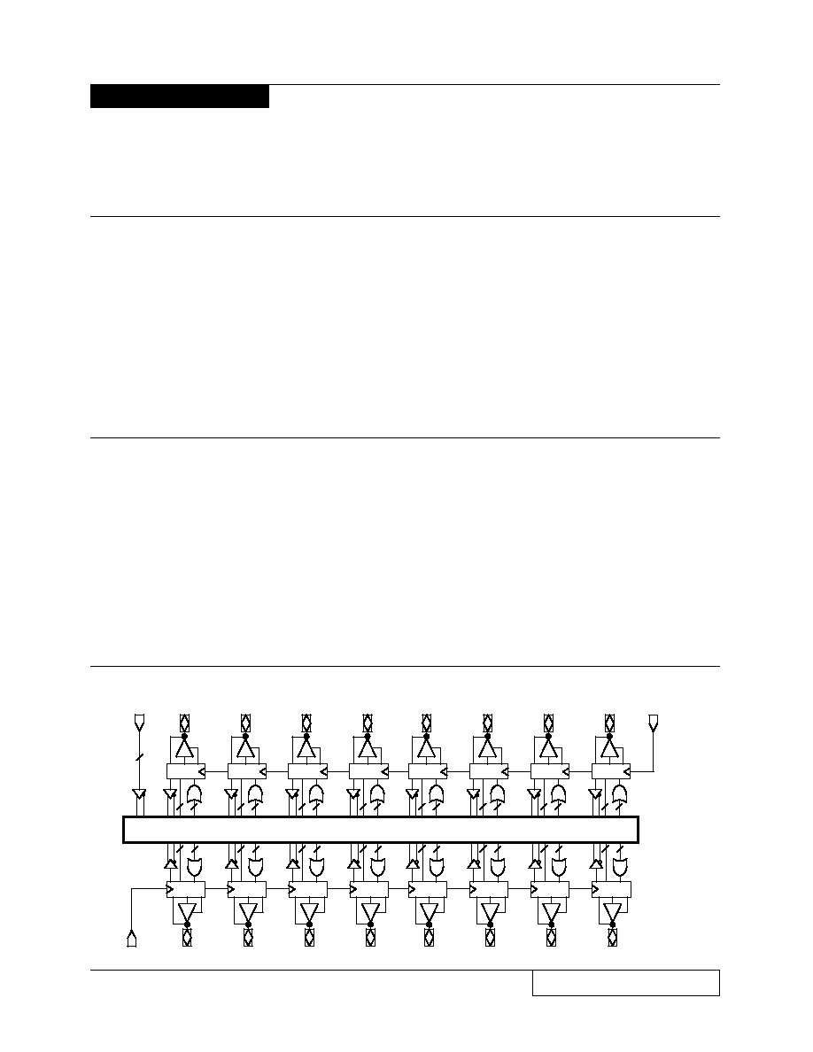
BLOCK DIAGRAM
4
2 8
CLK2
12950G-1
I
I/O16
CLK1
2 8
I/O15
2 8
I/O14
I/O13
2 8
I/O12
I/O11
I/O10
I/O9
2 8
I/O8
2 8
I/O7
2 8
I/O6
2 8
I/O5
2 8
I/O4
2 8
I/O3
2 8
I/O2
2 8
I/O1
Programmable AND Array
40 x 160
Lattice Semiconductor
USE GAL DEVICES FOR NEW DESIGNS
相關(guān)PDF資料 |
PDF描述 |
|---|---|
| PALCE610H-15JC | USE GAL DEVICES FOR NEW DESIGNS |
| PALCE610H-15PC | USE GAL DEVICES FOR NEW DESIGNS |
| PALCE610H-25 | USE GAL DEVICES FOR NEW DESIGNS |
| PALCE610 | USE GAL DEVICES FOR NEW DESIGNS |
| PALCE610H-15 | USE GAL DEVICES FOR NEW DESIGNS |
相關(guān)代理商/技術(shù)參數(shù) |
參數(shù)描述 |
|---|---|
| PALE22V10-7JC | 制造商: 功能描述: 制造商:undefined 功能描述: |
| PalExpert | 功能描述:開發(fā)軟件 RoHS:否 制造商:Atollic Inc. 產(chǎn)品:Compilers/Debuggers 用于:ARM7, ARM9, Cortex-A, Cortex-M, Cortex-R Processors |
| PA-LF256/5384VE | 功能描述:插座和適配器 256-P fpBGA Skt Adp ispLSI 5384VE RoHS:否 制造商:Silicon Labs 產(chǎn)品:Adapter 用于:EM35x |
| PALF30807F | 制造商:Panasonic Industrial Company 功能描述:TRANSFORMER |
| PALF34602F | 制造商:Panasonic Industrial Company 功能描述:TRANSFORMER |
發(fā)布緊急采購,3分鐘左右您將得到回復(fù)。