- 您現(xiàn)在的位置:買(mǎi)賣IC網(wǎng) > PDF目錄369946 > PALLV16V8-10SC (LATTICE SEMICONDUCTOR CORP) Low Voltage, Zero Power 20-Pin EE CMOS Universal Programmable Array Logic PDF資料下載
參數(shù)資料
| 型號(hào): | PALLV16V8-10SC |
| 廠商: | LATTICE SEMICONDUCTOR CORP |
| 元件分類: | PLD |
| 英文描述: | Low Voltage, Zero Power 20-Pin EE CMOS Universal Programmable Array Logic |
| 中文描述: | EE PLD, 10 ns, PDSO20 |
| 封裝: | PLASTIC, SOIC-20 |
| 文件頁(yè)數(shù): | 3/22頁(yè) |
| 文件大小: | 425K |
| 代理商: | PALLV16V8-10SC |
第1頁(yè)第2頁(yè)當(dāng)前第3頁(yè)第4頁(yè)第5頁(yè)第6頁(yè)第7頁(yè)第8頁(yè)第9頁(yè)第10頁(yè)第11頁(yè)第12頁(yè)第13頁(yè)第14頁(yè)第15頁(yè)第16頁(yè)第17頁(yè)第18頁(yè)第19頁(yè)第20頁(yè)第21頁(yè)第22頁(yè)

PALLV16V8-10 and PALLV16V8Z-20 Families
3
The user is given two design options with the PALLV16V8. First, it can be programmed as a
standard PAL device from the PAL16R8 and PAL10H8 series. The PAL programmer manufacturer
will supply device codes for the standard PAL device architectures to be used with the PALLV16V8.
The programmer will program the PALLV16V8 in the corresponding architecture. This allows the
user to use existing standard PAL device JEDEC files without making any changes to them.
Alternatively, the device can be programmed as a PALLV16V8. Here the user must use the
PALLV16V8 device code. This option allows full utilization of the macrocell.
CONFIGURATION OPTIONS
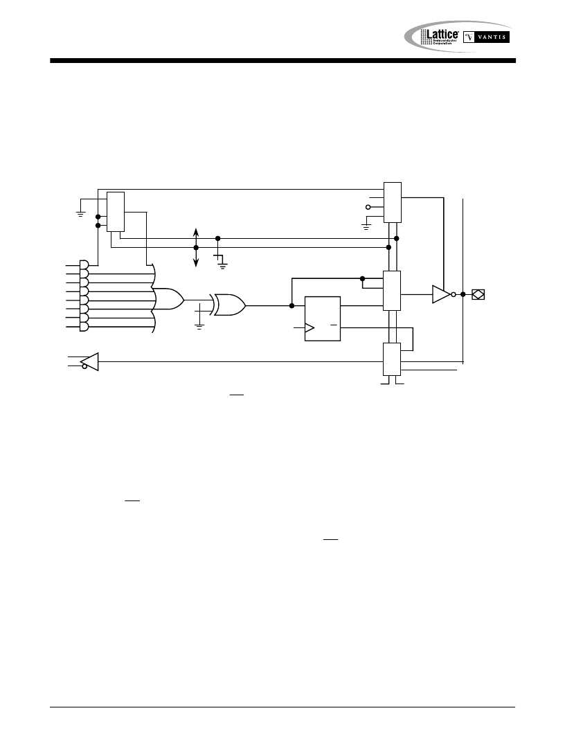
Each macrocell can be configured as one of the following: registered output, combinatorial output,
combinatorial I/O, or dedicated input. In the registered output configuration, the output buffer is
enabled by the OE pin. In the combinatorial configuration, the buffer is either controlled by a
product term or always enabled. In the dedicated input configuration, it is always disabled. With
the exception of MC
0
and MC
7
, a macrocell configured as a dedicated input derives the input signal
from an adjacent I/O. MC
0
derives its input from pin 11 (OE) and MC
The macrocell configurations are controlled by the configuration control word. It contains 2 global
bits (SG0 and SG1) and 16 local bits (SL0
0
through SL0
whether registers will be allowed. SG1 determines whether the PALLV16V8 will emulate a PAL16R8
family. Within each macrocell, SL0
x
, in conjunction with SG1, selects the configuration of the
macrocell, and SL1
x
sets the output as either active low or active high for the individual macrocell.
The configuration bits work by acting as control inputs for the multiplexers in the macrocell. There
are four multiplexers: a product term input, an enable select, an output select, and a feedback
select multiplexer. SG1 and SL0
x
are the control signals for all four multiplexers. In MC
7
from pin 1 (CLK).
7
and SL1
0
through SL1
7
). SG0 determines
0
and MC
7
,
1 0
0 1
17713D-004
*In macrocells MC
0
and MC
7
,
SG1 is replaced by SG0 on the feedback multiplexer.
1 1
0 X
*SG1
SG1
SL0
X
D
Q
Q
1 0
1 1
0 X
1 1
1 0
0 0
V
CC
CLK
SL0
X
OE
To
Adjacent
Macrocell
From
Adjacent
Pin
1 1
0 X
1 0
SL1
X
I/O
X
Figure 1. PALLV16V8 Macrocell
相關(guān)PDF資料 |
PDF描述 |
|---|---|
| PAN4820 | On-board type DC Noise Filter for Telecom |
| PAQ65D48 | Dual output DC-DC power module for TELECOM |
| PAQ65D48-3325 | Dual output DC-DC power module for TELECOM |
| PAQ65D48-5033 | Dual output DC-DC power module for TELECOM |
| PAQ65D48-2518 | Dual output DC-DC power module for TELECOM |
相關(guān)代理商/技術(shù)參數(shù) |
參數(shù)描述 |
|---|---|
| PALLV16V8Z-20JI | 制造商: 功能描述: 制造商:undefined 功能描述: |
| PALLV16V8Z-20PI | 制造商:Rochester Electronics LLC 功能描述:- Bulk 制造商:Advanced Micro Devices 功能描述:Simple E2PLD, Programmable Array Logic, 20 Pin, Plastic, DIP 制造商:Lattice Semiconductor Corporation 功能描述: |
| PALLV16V8Z-20SI | 制造商:未知廠家 制造商全稱:未知廠家 功能描述:Electrically-Erasable PLD |
| PALLV16V8Z-25JI | 制造商:未知廠家 制造商全稱:未知廠家 功能描述:Electrically-Erasable PLD |
| PALLV16V8Z-25PI | 制造商:未知廠家 制造商全稱:未知廠家 功能描述:Electrically-Erasable PLD |
發(fā)布緊急采購(gòu),3分鐘左右您將得到回復(fù)。