- 您現(xiàn)在的位置:買賣IC網(wǎng) > PDF目錄367822 > PCIB40 PC(ISA)BUS I/O CARD PDF資料下載
參數(shù)資料
| 型號(hào): | PCIB40 |
| 英文描述: | PC(ISA)BUS I/O CARD |
| 中文描述: | 電腦(ISA)總線的I / O卡 |
| 文件頁數(shù): | 5/16頁 |
| 文件大小: | 284K |
| 代理商: | PCIB40 |
2192-09066-000-000
Counter Timers
The PCIB40 includes three programmable 16-bit counter/timers. Counter 0 may be driven by either
a 10KHz, 100KHz or 1MHz clock and can be used to generate regular interrupts. An interrupt is
generated
only
when the counter 0 output goes to a ‘1’.
The input and gate control signals of counters 1 and 2 are connected as inputs from the D-50 while
the counter outputs are linkable to the D-50 connector. Counter inputs 1 and 2 may be used for
frequency or pulse measurement and the outputs used for pulse generation. Refer to the link
section and pin assignments table for connection details.
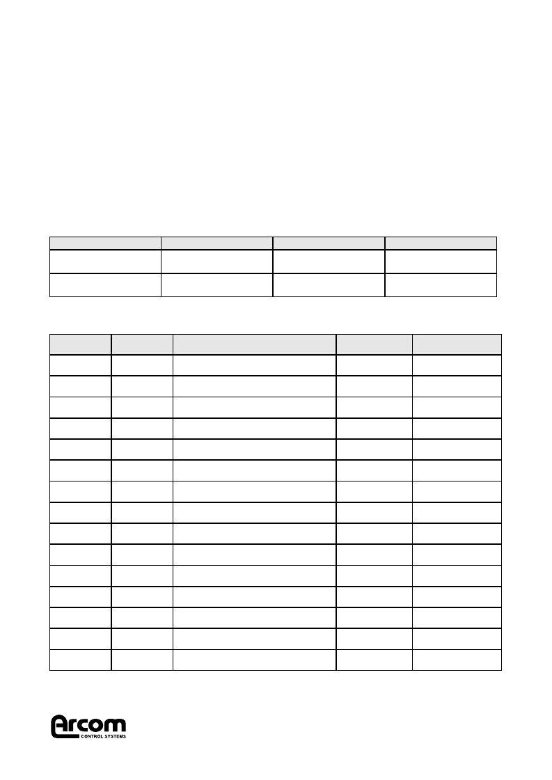
I/O map
The value written to the pointer register is used to select the on-board I/O location to be accessed.
This board occupies two consecutive addresses and has nine I/O function registers and three
special function registers.
The board must be set on an
even
address boundary. (i.e. 180h, 182h, 200h etc.)
I/O Function Registers
* A copy of the 8254 (71054) data sheet may be obtained from our Customer Support team (Tel: 01223 412 428)
J206 PCIB40 Technical Manual
5
Address
Base (180h)
Write Only
Pointer Register
On-board register
(e.g. 80h)
Data to Read/Write
from/to register
Base+1 (181H)
Read/Write
Data Register
Read/write
Register Name
Register Function
Pointer Value
(hex)
00
Write
Read
Write
Read
Write
Read
Write
Read
Write
Read
Read/Write
Read/Write
Read/Write
Write
Output Control Latches Group 0
Bit 0-7
0= Output ‘0’
1= Output ‘1’
0= Input ‘0’
1= Input ‘1’
0= Output ‘0’
1= Output ‘1’
0= Input ‘0’
1= Input ‘1’
0= Output ‘0’
1= Output ‘1’
0= Input ‘0’
1= Input ‘1’
0= Output ‘0’
1= Output ‘1’
0= Input ‘0’
1= Input ‘1’
0= Output ‘0’
1= Output ‘1’
0= Input ‘0’
1= Input ‘1’
See data sheet 8254*
See data sheet 8254*
See data sheet 8254*
See data sheet 8254*
Bit 0-7
Bit 0-7
Bit 0-7
Bit 0-7
Bit 0-7
Bit 0-7
Bit 0-7
Bit 0-7
Bit 0-7
Bit 0-7
Bit 0-7
Bit 0-7
Bit 0-7
Status of Group 0
Output Control Latches Group 1
Status of Group 1
Output Control Latches Group 2
Status of Group 2
Output Control Latches Group 3
Status of Group 3
Output Control Latches Group 4
Status of Group 4
Not Used
Counter/timer 0 Access
Counter/timer 1 Access
Counter/timer 2 Access
Counter/Timer Control Word
00
01
01
02
02
03
03
04
04
05 - 0F
10
11
12
13
Read/Write
Pointer Name
Pointer Bit
Functions
相關(guān)PDF資料 |
PDF描述 |
|---|---|
| PCICLOCKGEN_R001 | AMD Alchemy? Solutions Au1500? PCI Clock Generation? |
| PCK2000 | CK97 (66/100MHz) System Clock Generator(CK97 (66/100MHz) 系統(tǒng)時(shí)鐘發(fā)生器) |
| PCK2000DL | CK97 66/100MHz System Clock Generator |
| PCK2001M | 14.318-150 MHz IIC 1:10 clock buffer(14.318-150 MHz IIC 1:10時(shí)鐘緩沖器) |
| PCK2001R | 14.318-133 MHz I2C 1:6 Clock Buffer(14.318-133 MHz I2C 1:6時(shí)鐘緩沖器) |
相關(guān)代理商/技術(shù)參數(shù) |
參數(shù)描述 |
|---|---|
| PCIC16W7M400C1 | 制造商:Positronic Industries 功能描述: |
| PCI-C588 | 功能描述:界面模塊 8 PORT ASYNC SERIAL COMM PCI CARD RoHS:否 制造商:4D Systems 產(chǎn)品:Serial Converters 通道/端口數(shù)量: 數(shù)據(jù)速率: 接口類型:USB, UART 工作電源電壓:3.3 V, 5 V 最大工作溫度: |
| PCI-C6600S4-2-67-167 | 制造商:Johnson Components 功能描述:SBC;DSP, 2 C9701, 2MB SRAM, IN |
| PCI-COM2 | 制造商:BCM Advanced Research 功能描述:2 PORT COM CARD - Bulk |
| PCI-COM4 | 制造商:BCM Advanced Research 功能描述:4 COM PORTS SERIAL CARD SUPPORTS 4 RX232/422/485 - Bulk |
發(fā)布緊急采購,3分鐘左右您將得到回復(fù)。