- 您現(xiàn)在的位置:買賣IC網(wǎng) > PDF目錄367860 > PDIUSBH12 (NXP Semiconductors N.V.) USB 2-port hub PDF資料下載
參數(shù)資料
| 型號(hào): | PDIUSBH12 |
| 廠商: | NXP Semiconductors N.V. |
| 英文描述: | USB 2-port hub |
| 中文描述: | 2的USB端口集線器 |
| 文件頁數(shù): | 18/28頁 |
| 文件大小: | 170K |
| 代理商: | PDIUSBH12 |
第1頁第2頁第3頁第4頁第5頁第6頁第7頁第8頁第9頁第10頁第11頁第12頁第13頁第14頁第15頁第16頁第17頁當(dāng)前第18頁第19頁第20頁第21頁第22頁第23頁第24頁第25頁第26頁第27頁第28頁
Philips Semiconductors
Product specification
PDIUSBH12
USB 2-port hub
1999 Jul 22
18
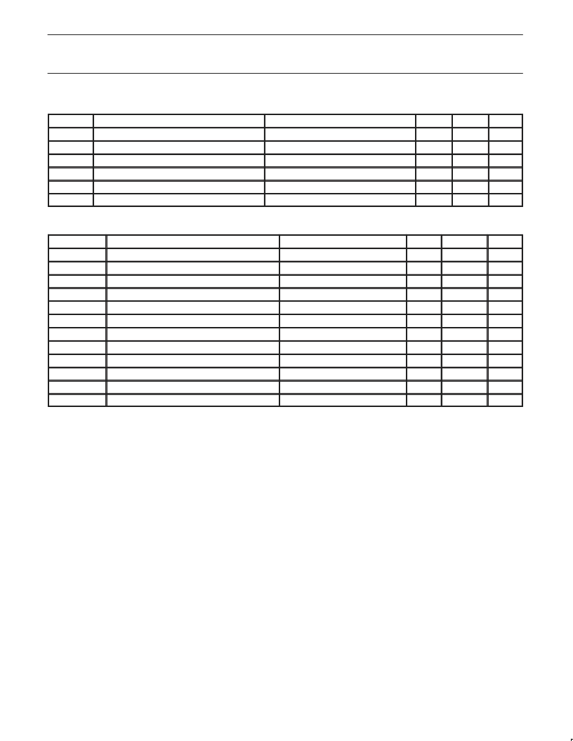
RECOMMENDED OPERATING CONDITIONS
SYMBOL
PARAMETER
TEST CONDITIONS
MIN
MAX
UNIT
V
CC
V
I
V
I/O
V
AI/O
V
O
T
amb
DC supply voltage
3.0
3.6
V
DC input voltage range
0
5.5
V
DC input voltage range for I/O
0
5.5
V
DC input voltage range for analog I/O
0
V
CC
V
CC
85
V
DC output voltage range
0
V
Operating ambient temperature range in free air
See DC and AC characteristics per device
–40
°
C
ABSOLUTE MAXIMUM RATINGS
1
SYMBOL
PARAMETER
TEST CONDITIONS
MIN
MAX
UNIT
V
CC
I
IK
V
I
V
I/O
I
OK
V
O
I
O
I
O
DC supply voltage
–0.5
+4.6
V
DC input diode current
V
I
< 0
Note 2
–50
mA
DC input voltage
–0.5
+5.5
V
DC input voltage range for I/O’s
–0.5
V
CC
+ 0.5
±
50
V
DC output diode current
V
O
> V
CC
or V
O
< 0
Note 2
mA
DC output voltage
–0.5
V
CC
+ 0.5
±
15
±
50
±
100
±
4000
4
V
DC output sink or source current for other pins
V
O
= 0 to V
CC
V
O
= 0 to V
CC
mA
DC output sink or source current for D+/D– pins
mA
I
GND
, I
CC
V
ESD
T
STG
P
TOT
NOTES:
1. Stresses beyond those listed may cause damage to the device. These are stress ratings only and functional operation of the device at these
or any other conditions beyond those listed in the RECOMMENDED OPERATING CONDITIONS table is not implied. Exposure to absolute
maximum rated conditions for extended periods may affect device reliability.
2. The input and output voltage ratings may be exceeded if the input and output current ratings are observed.
3. Values are given for device only: in-circuit V
ESD(MAX)
=
±
8000 V.
4. For open-drain pins V
ESD(MAX)
=
±
2000 V.
DC V
CC
or GND current
Electrostatic discharge voltage
mA
I
IL
< 1
μ
A
3
—
V
Storage temperature range
–60
+150
°
C
Power dissipation per package
相關(guān)PDF資料 |
PDF描述 |
|---|---|
| PDIUSBH12D | USB 2-port hub |
| PDIUSBH12N | USB 2-port hub |
| PDIUSBP11A | Universal Serial Bus Transceiver(通用串行總線收發(fā)器) |
| PDUSBP11APWDH | Universal Serial Bus Transceiver |
| PDIUSBP11AD | Universal Serial Bus Transceiver |
相關(guān)代理商/技術(shù)參數(shù) |
參數(shù)描述 |
|---|---|
| PDIUSBH12D | 制造商:PHILIPS 制造商全稱:NXP Semiconductors 功能描述:USB 2-port hub |
| PDIUSBH12N | 制造商:PHILIPS 制造商全稱:NXP Semiconductors 功能描述:USB 2-port hub |
| PDIUSBH12NB | 制造商:未知廠家 制造商全稱:未知廠家 功能描述:BUS CONTROLLER |
| PDIUSBP11 | 制造商:PHILIPS 制造商全稱:NXP Semiconductors 功能描述:Universal Serial Bus transceiver |
| PDIUSBP11A | 制造商:PHILIPS 制造商全稱:NXP Semiconductors 功能描述:Universal Serial Bus Transceiver |
發(fā)布緊急采購,3分鐘左右您將得到回復(fù)。