- 您現(xiàn)在的位置:買賣IC網(wǎng) > PDF目錄367902 > PECL_RX_C3 (AUSTRIAMICROSYSTEMS AG) CMOS PECL Receiver PDF資料下載
參數(shù)資料
| 型號: | PECL_RX_C3 |
| 廠商: | AUSTRIAMICROSYSTEMS AG |
| 英文描述: | CMOS PECL Receiver |
| 中文描述: | PECL的接收機的CMOS |
| 文件頁數(shù): | 5/6頁 |
| 文件大小: | 280K |
| 代理商: | PECL_RX_C3 |
Datasheet:PECL_RX - C35
RevisionB,10.09.02
Page5fo6
APPLICATION
!
!
!
!
!
HighSpeedBackplaneDriver
ComplementaryClockDrivers
LevelTranslator
SystemInterconnects
ATMApplications
!
!
!
!
SDHApplications
High-ResolutionImagingApplications
LaserPrinters
DigitalCopiers
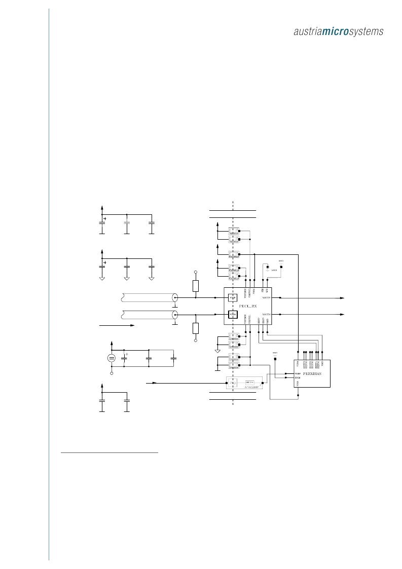
TYPICAL APPLICATION
1)
μ
F
1
μ
F
1
VDDA
VSSA
22pF
100pF
VREF (external reference)
2)
SNAP BACK
6)
50
3)
μ
F
1
22pF
100pF
VDDA
VT
-
2V
VREF
VSSA
3)
180pF
1nF
50
50
+
external
chip internal
VDD
4)
VDDA
1)
1)4)
VDDA
SNAP BACK
6)
VSS
4)
3)
VSSA
4)
3)
7)
7)
7)
5)
complementary
CMOS signals
(to digital core)
VDD
VSS
3)
22pF
100pF
DATA
transmission lines
from transmitter
DATAN
VT
VT
1)
2)
3)
4)
5)
6)
7)
Eachpowerpinmusthaveitsownsetofblockingcapacitors.
Anexternalreferencemustbeused.
VSSAandVSS mustbeconnectedonthePCBlevel.
Thetwopowerpadscanbebondedtoonepackagepin(doublebonding).
TwomorePECL_RX cellscanbedrivenwithIREFxxofthePERXBIAS cell.IfanoutputIREFxxisnotuseditmustbeleftunconnected.
ThePECLpartofthechiphastobeseparatedfromtherestofthechipbyuseofsnapbacks(cellPWRCUT_DIG_P_SNAP_SNAP).
ThecellsVDD3R1PandVDD3R2Parenotinthestandardlibrary, theyarepartoftheIP-block.
相關PDF資料 |
PDF描述 |
|---|---|
| PECL10-3 | Logic IC |
| PECL10-4 | Logic IC |
| PECL15-2 | Logic IC |
| PECL15-3 | LTC3525ESC6-3.3 Evaluation Kit |
| PECL15-4 | Logic IC |
相關代理商/技術(shù)參數(shù) |
參數(shù)描述 |
|---|---|
| PECO-17S | 制造商:PMA 功能描述:20MM NYLON GRY CONT. PACK |
| PECO-23B | 制造商:PMA 功能描述:25MM NYLON BLK CONT. PACK |
| PECS0DBX0 | 制造商:TE Connectivity 功能描述: |
| PECS0DHX0 | 制造商:TE Connectivity 功能描述: |
| PECS0SHX0 | 制造商:TE Connectivity 功能描述: |
發(fā)布緊急采購,3分鐘左右您將得到回復。