- 您現(xiàn)在的位置:買賣IC網(wǎng) > PDF目錄367941 > PHB13N40E (NXP SEMICONDUCTORS) PowerMOS transistors Avalanche energy rated PDF資料下載
參數(shù)資料
| 型號(hào): | PHB13N40E |
| 廠商: | NXP SEMICONDUCTORS |
| 元件分類: | JFETs |
| 英文描述: | PowerMOS transistors Avalanche energy rated |
| 中文描述: | 13.7 A, 400 V, 0.35 ohm, N-CHANNEL, Si, POWER, MOSFET |
| 封裝: | SOT-404, 3 PIN |
| 文件頁數(shù): | 2/10頁 |
| 文件大?。?/td> | 104K |
| 代理商: | PHB13N40E |
Philips Semiconductors
Product specification
PowerMOS transistors
Avalanche energy rated
PHP13N40E, PHB13N40E, PHW13N40E
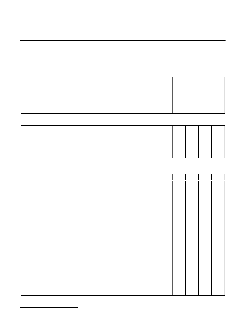
AVALANCHE ENERGY LIMITING VALUES
Limiting values in accordance with the Absolute Maximum System (IEC 134)
SYMBOL PARAMETER
E
AS
Non-repetitive avalanche
energy
CONDITIONS
Unclamped inductive load, I
= 13.6 A;
t
p
= 0.2 ms; T
j
prior to avalanche = 25C;
V
DD
≤
50 V; R
GS
= 50
; V
GS
= 10 V
MIN.
-
MAX.
705
UNIT
mJ
E
AR
Repetitive avalanche energy
2
I
= 13.7 A; t
= 2.5
μ
s; T
avalanche = 25C; R
GS
= 50
; V
GS
= 10 V
Repetitive and non-repetitive
avalanche current
-
18
mJ
I
AS
, I
AR
-
13.7
A
THERMAL RESISTANCES
SYMBOL PARAMETER
R
th j-mb
Thermal resistance junction
to mounting base
R
th j-a
Thermal resistance junction
to ambient
CONDITIONS
MIN.
-
TYP. MAX. UNIT
-
0.8
K/W
SOT78 package, in free air
SOT429 package, in free air
SOT404 package, pcb mounted, minimum
footprint
-
-
-
60
45
50
-
-
-
K/W
K/W
K/W
ELECTRICAL CHARACTERISTICS
T
j
= 25 C unless otherwise specified
SYMBOL PARAMETER
V
(BR)DSS
Drain-source breakdown
voltage
V
(BR)DSS
/ Drain-source breakdown
T
j
voltage temperature
coefficient
R
DS(ON)
Drain-source on resistance
V
GS(TO)
Gate threshold voltage
g
fs
Forward transconductance
I
DSS
Drain-source leakage current V
DS
= 400 V; V
GS
= 0 V
CONDITIONS
V
GS
= 0 V; I
D
= 0.25 mA
MIN.
400
TYP. MAX. UNIT
-
-
V
V
DS
= V
GS
; I
D
= 0.25 mA
-
0.1
-
%/K
V
GS
= 10 V; I
= 6.5 A
V
DS
= V
; I
D
= 0.25 mA
V
DS
= 30 V; I
= 6.5 A
-
0.26
3.0
7.5
1
50
10
79
7.2
43
16
40
100
42
3.5
4.5
0.35
4.0
-
25
500
200
100
12
55
-
-
-
-
-
-
V
S
μ
A
μ
A
nA
nC
nC
nC
ns
ns
ns
ns
nH
nH
2.0
4
-
-
-
-
-
-
-
-
-
-
-
-
V
DS
= 320 V; V
GS
= 0 V; T
j
= 125 C
I
GSS
Q
g(tot)
Q
gs
Q
gd
t
d(on)
t
r
t
d(off)
t
f
L
d
L
d
Gate-source leakage current V
GS
=
±
30 V; V
DS
= 0 V
Total gate charge
Gate-source charge
Gate-drain (Miller) charge
Turn-on delay time
Turn-on rise time
Turn-off delay time
Turn-off fall time
Internal drain inductance
Internal drain inductance
I
D
= 13 A; V
DD
= 320 V; V
GS
= 10 V
V
DD
= 200 V; R
D
= 15
;
R
G
= 5.6
Measured from tab to centre of die
Measured from drain lead to centre of die
(SOT78 package only)
Measured from source lead to source
bond pad
V
GS
= 0 V; V
DS
= 25 V; f = 1 MHz
L
s
Internal source inductance
-
7.5
-
nH
C
iss
C
oss
C
rss
Input capacitance
Output capacitance
Feedback capacitance
-
-
-
1283
218
120
-
-
-
pF
pF
pF
2
pulse width and repetition rate limited by T
j
max.
December 1998
2
Rev 1.000
相關(guān)PDF資料 |
PDF描述 |
|---|---|
| PHW13N40E | PowerMOS transistors Avalanche energy rated |
| PHP176NQ04T | N-channel TrenchMOS-TM standard level FET |
| PHP1N60E | PowerMOS transistor |
| PHP206 | Dual P-channel enhancement mode MOS transistor |
| PHP33N10 | PowerMOS transistor(功率MOS晶體管) |
相關(guān)代理商/技術(shù)參數(shù) |
參數(shù)描述 |
|---|---|
| PHB143NQ04T /T3 | 功能描述:MOSFET TRENCHMOS (TM)FET RoHS:否 制造商:STMicroelectronics 晶體管極性:N-Channel 汲極/源極擊穿電壓:650 V 閘/源擊穿電壓:25 V 漏極連續(xù)電流:130 A 電阻汲極/源極 RDS(導(dǎo)通):0.014 Ohms 配置:Single 最大工作溫度: 安裝風(fēng)格:Through Hole 封裝 / 箱體:Max247 封裝:Tube |
| PHB143NQ04T,118 | 功能描述:MOSFET TRENCHMOS (TM)FET RoHS:否 制造商:STMicroelectronics 晶體管極性:N-Channel 汲極/源極擊穿電壓:650 V 閘/源擊穿電壓:25 V 漏極連續(xù)電流:130 A 電阻汲極/源極 RDS(導(dǎo)通):0.014 Ohms 配置:Single 最大工作溫度: 安裝風(fēng)格:Through Hole 封裝 / 箱體:Max247 封裝:Tube |
| PHB145NQ06T,118 | 功能描述:MOSFET TRENCHMOS (TM) FET RoHS:否 制造商:STMicroelectronics 晶體管極性:N-Channel 汲極/源極擊穿電壓:650 V 閘/源擊穿電壓:25 V 漏極連續(xù)電流:130 A 電阻汲極/源極 RDS(導(dǎo)通):0.014 Ohms 配置:Single 最大工作溫度: 安裝風(fēng)格:Through Hole 封裝 / 箱體:Max247 封裝:Tube |
| PHB146NQ06LT | 制造商:PHILIPS 制造商全稱:NXP Semiconductors 功能描述:N-channel TrenchMOS logic level FET |
| PHB146NQ06LT,118 | 功能描述:MOSFET TRENCHMOS (TM) FET RoHS:否 制造商:STMicroelectronics 晶體管極性:N-Channel 汲極/源極擊穿電壓:650 V 閘/源擊穿電壓:25 V 漏極連續(xù)電流:130 A 電阻汲極/源極 RDS(導(dǎo)通):0.014 Ohms 配置:Single 最大工作溫度: 安裝風(fēng)格:Through Hole 封裝 / 箱體:Max247 封裝:Tube |
發(fā)布緊急采購,3分鐘左右您將得到回復(fù)。