- 您現(xiàn)在的位置:買(mǎi)賣(mài)IC網(wǎng) > PDF目錄368010 > PI74FCT163245 (Pericom Semiconductor Corp.) Fast CMOS 3.3V 16-Bit Bidirectional Transceiver PDF資料下載
參數(shù)資料
| 型號(hào): | PI74FCT163245 |
| 廠商: | Pericom Semiconductor Corp. |
| 英文描述: | Fast CMOS 3.3V 16-Bit Bidirectional Transceiver |
| 中文描述: | 快速CMOS 3.3V的16位雙向收發(fā)器 |
| 文件頁(yè)數(shù): | 1/5頁(yè) |
| 文件大小: | 57K |
| 代理商: | PI74FCT163245 |
PI74FCT163245
3.3V 16-BIT BIDIRECTIONAL TRANSCEIVER
1
PS2054B 01/18/99
12345678901234567890123456789012123456789012345678901234567890121234567890123456789012345678901212345678901234567890123456789012123456789012
Product Description
Pericom Semiconductor’s PI74FCT series of logic circuits are
produced in the Company’s advanced 0.6 micron CMOS
technology, achieving industry leading speed grades.
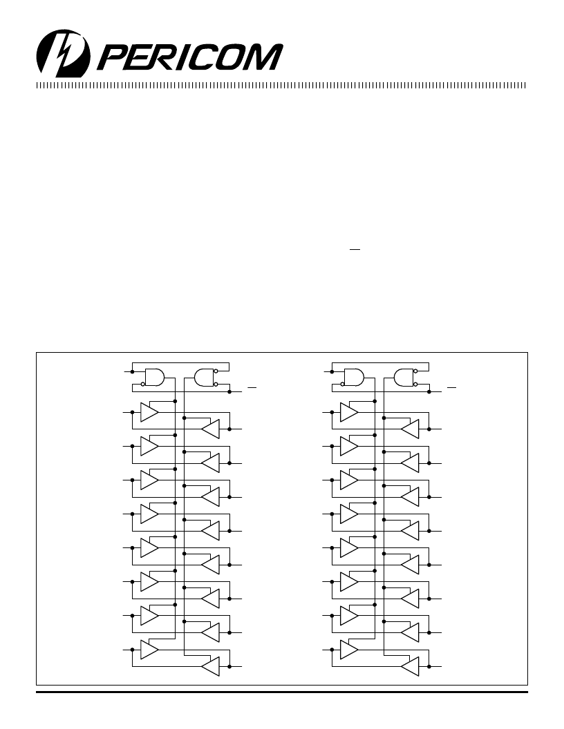
The PI74FCT163245 is a 16-bit bidirectional transceiver designed
for asynchronous two-way communication between data buses.
The direction control input pin (xDIR) determines the direction of
data flow through the bidirectional transceiver. The Direction and
Output Enable controls are designed to operate this device as either
two independent 8-bit transceivers or one 16-bit transceiver. The
output enable (xOE) input, when HIGH, disables both A and B
ports by placing them in HIGH Z condition.
12345678901234567890123456789012123456789012345678901234567890121234567890123456789012345678901212345678901234567890123456789012123456789012
12345678901234567890123456789012123456789012345678901234567890121234567890123456789012345678901212345678901234567890123456789012123456789012
PI74FCT163245
Fast CMOS 3.3V 16-Bit
Bidirectional Transceiver
Product Features
Advanced Low Power CMOS Operation
Excellent output drive capability:
Balanced drives (24mA sink and source)
Compatible with LVC
TM
class of products.
Pin compatible with industry standard double-density pinouts
Low ground bounce outputs
Hysteresis on all inputs
Industrial operating temperature range: –40°C to +85°C
Control inputs can be driven by 3.3V or 5V devices
Multiple center pin and distributed Vcc/GND pins
minimizing switching noise
Packages available:
– 48-pin 240 mil wide plastic TSSOP (A)
– 48-pin 300 mil wide plastic SSOP (V)
– 48-pin 173 mil wide plastic TVSOP (K)
Device models available on request
1
B
0
1
A
0
1
OE
1
DIR
1
B
1
1
A
1
1
B
2
1
A
2
1
B
3
1
A
3
1
B
4
1
A
4
1
B
5
1
A
5
1
B
6
1
A
6
1
B
7
1
A
7
2
B
0
2
A
0
2
OE
2
DIR
2
B
1
2
A
1
2
B
2
2
A
2
2
B
3
2
A
3
2
B
4
2
A
4
2
B
5
2
A
5
2
B
6
2
A
6
2
B
7
2
A
7
Logic Block Diagram
相關(guān)PDF資料 |
PDF描述 |
|---|---|
| PI74FCT163374 | Fast CMOS 3.3V 16-Bit Register (3-State) |
| PI74FCT2244ATH | Fast CMOS Octal Buffer/Line Drivers |
| PI74FCT244CTQ | Fast CMOS Octal Buffer/Line Drivers |
| PI74FCT244CTS | Fast CMOS Octal Buffer/Line Drivers |
| PI74FCT244DTQ | Fast CMOS Octal Buffer/Line Drivers |
相關(guān)代理商/技術(shù)參數(shù) |
參數(shù)描述 |
|---|---|
| PI74FCT163245A | 制造商:未知廠家 制造商全稱(chēng):未知廠家 功能描述:Dual 8-bit Bus Transceiver |
| PI74FCT163245AA | 制造商:Pericom Semiconductor Corporation 功能描述:Bus XCVR Dual 16-CH 3-ST 48-Pin TSSOP Tube |
| PI74FCT163245AK | 制造商:未知廠家 制造商全稱(chēng):未知廠家 功能描述:Dual 8-bit Bus Transceiver |
| PI74FCT163245ATA | 制造商:未知廠家 制造商全稱(chēng):未知廠家 功能描述:Dual 8-bit Bus Transceiver |
| PI74FCT163245ATV | 制造商:未知廠家 制造商全稱(chēng):未知廠家 功能描述:Dual 8-bit Bus Transceiver |
發(fā)布緊急采購(gòu),3分鐘左右您將得到回復(fù)。